

October 2024
Huawei begins trials in 7nm, AMD iterates across its whole roadmap at once, and Nvidia makes changes to its chips and racks.

(Want to see next month’s edition early? Follow this GitHub repo for the latest updates and early looks at the newsletter as it’s written - Also check out my LinkedIn!)
This month’s updates:
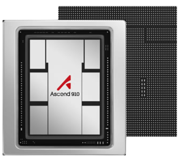
Huawei's Ascend 910C begins customer trials in China
Nvidia cancels the NVL 36x2 copper connected rack SKU
Nvidia moving away from SXM, starting with the rumoured “B300”
AMD announces Turin CPU, MI325X GPU, and a UEC-compliant NIC
Rumoured: Nvidia Vera/Rubin and Intel Falcon shores specs
One-pagers:
Instruction sets
Systolic arrays
Caches
This month's updates:
Huawei's Ascend 910C
Amidst the turmoil of Nvidia/TSMC Blackwell manufacturing delays, U.S. export controls, SMIC’s shaky 7nm process and incredible competition between various Chinese GPU manufacturers, how will Huawei’s Ascend series’ latest device, the 910C, compete?
U.S. export controls on semiconductor technology have forced Nvidia to make numerous changes to its AI-focused GPUs aimed at the enormous Chinese market, however there are rumours that another round of even tighter restrictions are about to hit. On top of this, China’s own SMIC is struggling to reliably produce chip dies at 7nm density, far behind TSMC/Intel/Samsung’s technologies. Multiple companies are competing to fill this AI training hardware vacuum in China, and Huawei has just begun sampling its Ascend 910C chip with customers, hoping for good results.
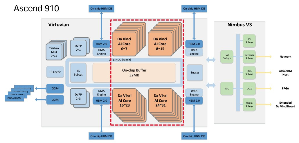
There isn’t much information on the specs of the 910C, but looking at what we know from our sources (1 2 3 4 5):
~512 TFLOPs (FP16) compute
96GB memory capacity
PCIe Gen5 socket (64GT/s/lane)
Supporting CXL 2.0 (64 GB/s)
Supporting multiple 200/400 GbE RoCE ports (on device, no separate NIC)
Manufactured with the SMIC 7nm process
HBM bandwidth of 2.4TB/s
600W TDP
Using proprietary HCCS for inter-chip
Nvidia cancels the NVL 36x2
Nvidia’s plans to sell the B100/200 series and their GB200 trays, as well as Quantum/Spectrum switches and their new NVLink switch all revolve around their NVL rack SKUs (1 2), which have just undergone another round of consolidation after some early customer feedback and industry sentiment analysis.
Recently, Nvidia announced 3 datacentre-ready recommended architectures, the NVL 36, 36x2 and 72. Of these, the NVL36 was clearly aimed at customers who are happy to sacrifice potential rack density for lower power per rack (~40kW) and the ability to use air cooling, and the NVL72 was aimed at those who wanted density at all costs, albeit incredible power draws of ~120-132kW- per rack and liquid cooling as a requirement. The NVL36x2 however, was a compromise that Nvidia has now determined was not going to generate sufficient demand.
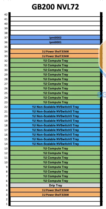
The key decision came down to one factor it seems: Energy efficiency. Both the 36 and 72-GPU racks each will have a CPU:GPU (Grace:Blackwell) ratio of 1:2 and hence the same compute trays, but crucially, the NV36x2 would need additional switching and cabling to support the NVLink copper interconnects between the GB200 compute servers on both racks, resulting a total power draw higher than a single NVL72, whilst being slightly less performant due to the increased switching and distances.
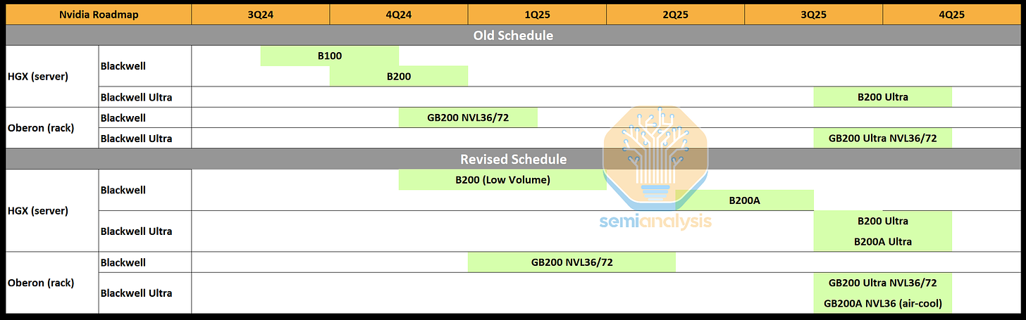
The revised schedule, likely to be updated again depending on early customer feedback in 1H2025. The x86 + Blackwell servers have not yet been announced but are likely on the way for 2H2025.
Nvidia moving away from SXM
The reason that NVidia’s GPUs have been able to have such high TDPs and use fast NVLink and C2C connections is due to SXM, their proprietary socket technology for putting GPUs onto the same board as CPUs and RAM. But this has, for a while now, caused issues that NVidia is now looking to fix with the GB300.
The Server PCIe Express Module (SXM) is proprietary NVidia tech for integrating a GPU into a baseboard (motherboard, main board, PCB, etc.), where other components like CPUs, RAM, and IO chips are connected. SXM, when released back in ~2016, solved many issues that NVidia were beginning to face and saw in their future. Using standard PCIe sockets to connect a power and memory bandwidth hungry GPU to a baseboard designed to handle components that were not as demanding, resulted in PCIe quickly becoming a problem.
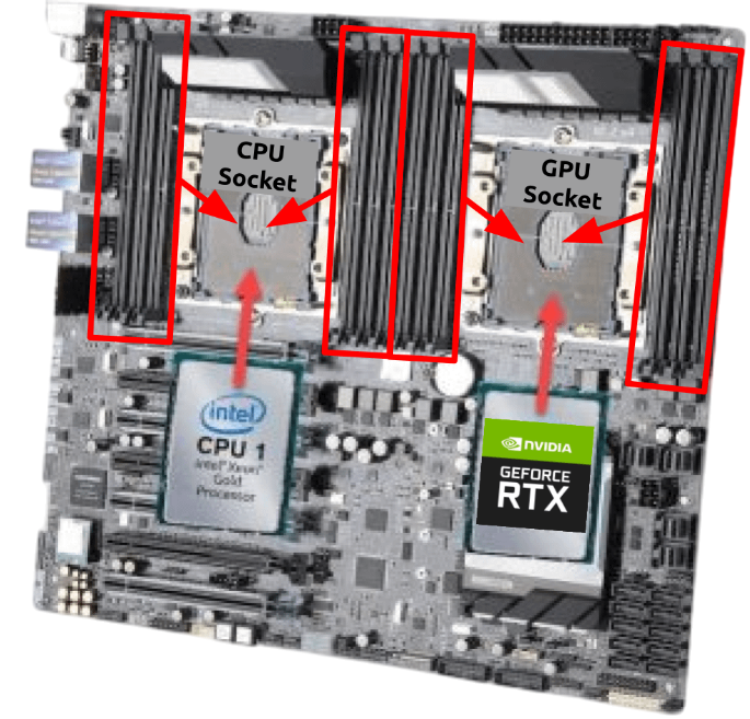
SXM solved this issue by integrating the GPU tighter (not as much as BGA, future discussion) into a custom baseboard, allowing for better power delivery to the device as well as enabling the use of the NVLink tech-stack to connect multiple GPUs on the same board and via NVSwitches to GPUs on other boards. Recently however, with GPUs being sold in the millions every year, the SXM sockets are causing issues for NVidia and OEMs with maintenance and after-sales support, as the tight bonding makes this difficult.

Rumours in the supply chain are that NVidia is considering moving to an independent socket design that will keep the benefits of SXM whilst making it easier to remove and replace GPUs on baseboards as well as making maintenance simpler. For ODMs that package GPU parts into cards like the H100 and so on, and OEMs that package cards into servers, this would simplify parts of their manufacturing processes as well as making aftersales repairs and upgrades easier. It's reported that the first product that this new socketing technology will be available for is the GB300, or what has been called the GB200 Ultra so far.
AMDs EPYC Turin, MI325X, and Pollara NIC
At their annual “Advancing AI” event AMD announced multiple new products to maintain its dominance (CPUs) and continue its push (GPUs and NICs) into the AI hardware market. Among these, the “Turin” CPU, MI325X GPU and Pollara NIC are the key names.
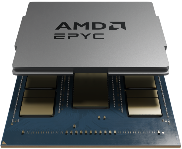
The AMD 5th gen CPU series, codenamed “Turin”, featuring AMDs Zen 5 architecture. Benchmarks are in and look good, but notably, Turin is not as big of an increase in performance from its predecessor as we have seen in the past. Multiple SKUs have been announced, with specs ranging from (1 2):
8 - 192 cores (1 – 2 sockets)
Up to 1.5TB of DDR5 RAM
Up to ~614 GB/s bandwidth
$527 - $14,813 per unit
64 – 512 MB L3 cache
Up to 5.0 GHz boost
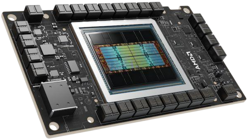
MI325X is a rather simple upgrade from the now famous MI300X, with all the specs being the same except for having more (and slightly better) HBM memory (192GB HBM3 -> 256GB HBM3e). As this competes with the Nvidia H200, it's understandable why AMD left the chip as it was and just added memory capacity (1 2):
256GB HBM3e (from 192GB HBM3)
6TB/s memory bandwidth (from 5.3TB/s)
1000W TDP (from 750W TDP)
1.3/2.6 PFLOPs FP16/FP8
128GB/s infinity fabric bandwidth (GPU-GPU + CPU-GPU)
~1.3x performance of H200 claimed
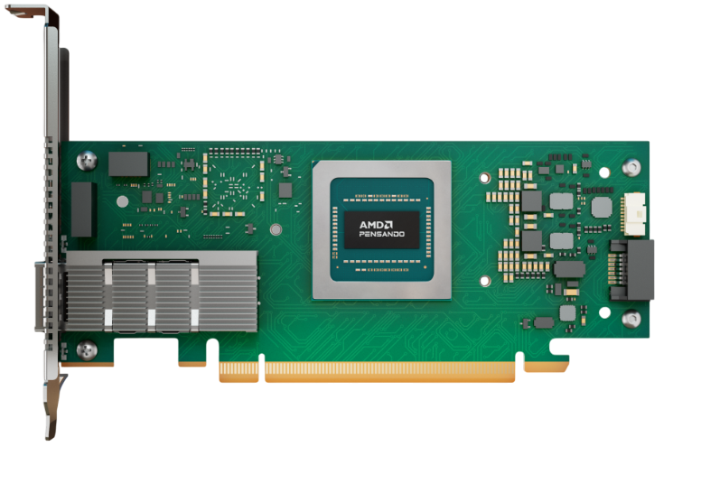
The Pensando series network interface card (NIC), codenamed “Pollara”, is the world's first NIC to support Ultra Ethernet, the new technology to consolidate RoCE and other optimisations and challenge (and open source) Inifiniband. Competing with the Nvidia (Mellanox) ConnectX-7, Pollara supports up to 1 x 400GbE (1):
4 x 100G / 2 x 200G / 1 x 400G support with QSFP112
Supports UEC optimisations and RoCEv2 compatible
PCIe Gen 5 x16 NIC-Host
(Rumours) Nvidia Vera/Rubin and Intel Falcon shores specs
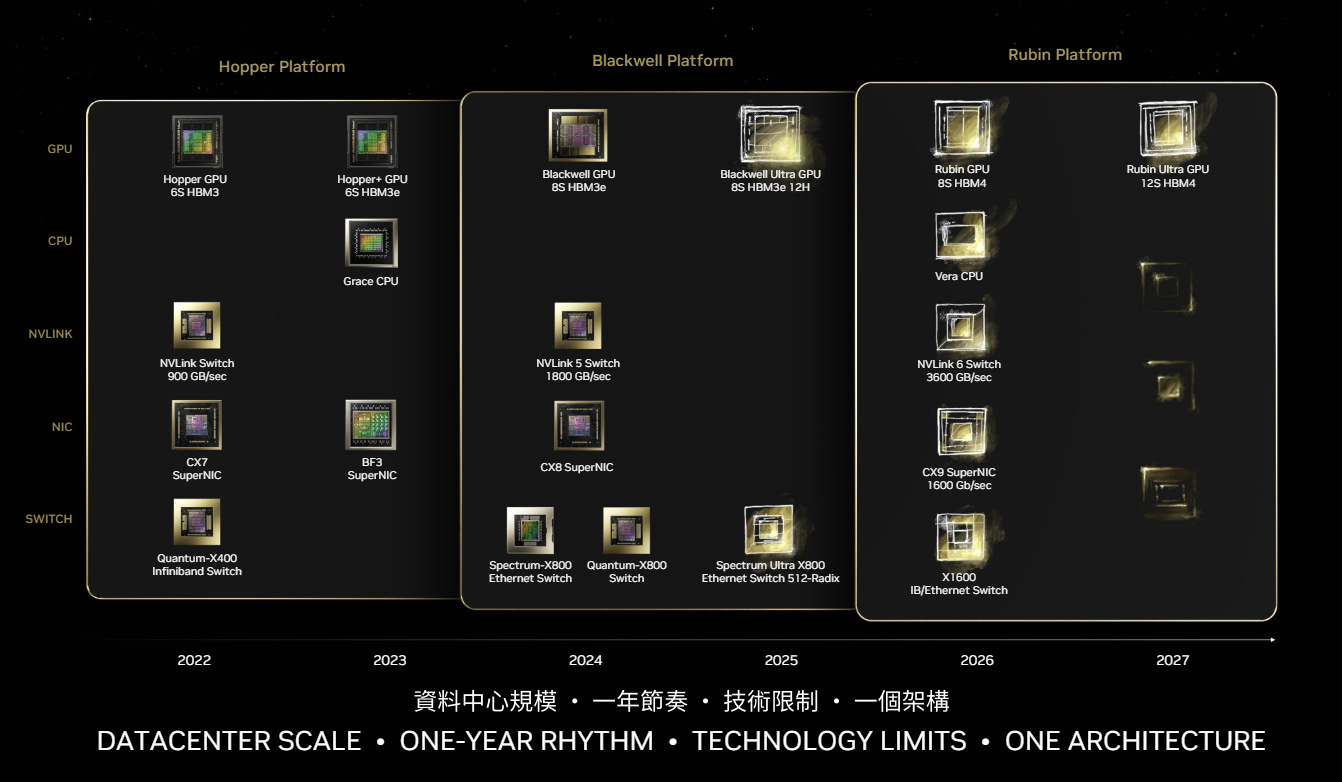
As we move towards 1Q2025, more and more leaks, reveals, and news finds its way into the public about next-next gen products (one after the next, announced, latest generation). Here we summarise what we know about the dates and specs of these products.
NVLink gen6 switch
3.6TB Agg. bi-directional bandwidth
CX9 SuperNIC
1.6TB/s single port bandwidth
X1600 switch (Ethernet AND InfiniBand):
1.6TB OSFP ports at a VERY high radix (512 likely)
Rubin GPU:
TDP competitive (1200W-1500W SXM/custom socket, 500W PCIe)
Using HBM4 8hi (1.6 TB/s per 48GB capacity device)
Vera CPU (ARM):
Likely C2C scales with NVLink (900GB/s bandwidth CPU-CPU/GPU)
Falcon shores CPU-GPU SoC:
TDP 1500W confirmed
Mixture of x86 CPU and Xe GPU
288GB HBM3, 9.8TB/s bandwidth
Using TSMC 3nm CoWoS-R not intel
Customisable CPU/GPU ratios
Absorbing Gaudi and Max series, maintaining backwards compatibility
Clearwater forest Xeon CPU:
Intel 18A process node
300 Billion transistors confirmed
Likely CXL 3.1 and UCIe 1.0/2.0 compatible
PCIe 6.0 ready
One-pagers:
Instruction sets
How does a CPU understand and carry out the calculations needed to run complex applications and workloads like AI or MS word? All these abstract and complex programs are broken down and compiled into lots of (relatively) simple, easy to understand instructions that the CPU can understand, called an instruction set.
The instruction set architecture (ISA) is a description of how to make use of a piece of complicated hardware like a CPU, at a very simple and straightforward level. In the diagram, 4 such instructions that almost all CPUs would understand are shown. These instructions describe what to do to data that is kept in certain parts of memory, R (registers), and where to put the result. For the ADD example, it's clear that the instruction states that the hardware should collect the numbers in R[s] and R[t], add them together, and put them in R[d].
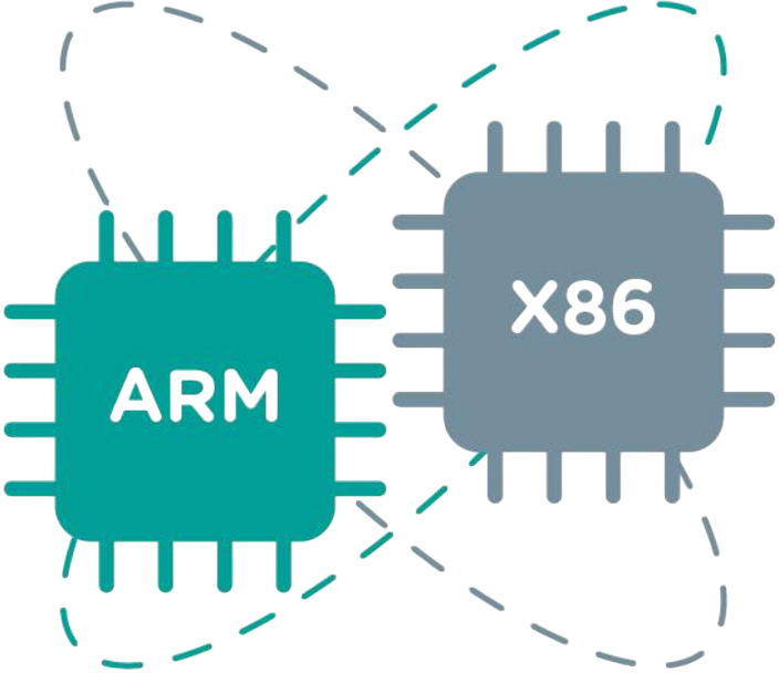
Of all the ISAs ever made for all the various hardware that exists out there, the two most popular for CPUs are x86 and ARM, both designed for general purpose compute and increasingly tuned over the years for higher and higher performance and efficiency.
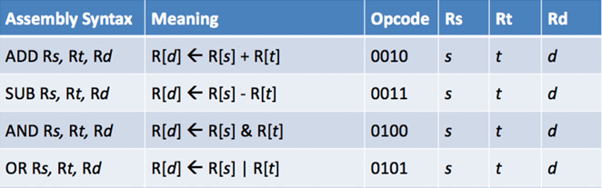
While x86 started on and continued down the path of being a complex instruction set computer (CISC), ARM was created to be a simpler, or “reduced” instruction set computer (RISC). Naturally, individual CISC instructions can perform a greater variety of more complicated transforms on source data, but also require more expensive and power-hungry hardware. In comparison, simpler individual instructions result in less complexity per individual instruction, requiring multiple simple instructions to do what one more complex instruction could do, but also require less expensive/complicated hardware and are generally more energy efficient.
Systolic arrays
The core computation that all current AI models are implemented as, the computation that our high-performing hardware has specialised to, for as long as we have been using compute for scientific purposes, is the matrix (array) multiplication. The most natural architecture to perform this is the systolic array.
The computations required to run almost all AI models are matrix multiplications (matmuls) - matrices just being a 2D array of numbers, and multiplying them being an operation between two matrices, A and B, to accumulate their information into a new third matrix, C, as shown in the diagram. When you can represent both the input data and the parameters of your AI model as matrices, it's clear why the matmul operation is key to enabling information propagation.

The systolic array is an architecture that acts as a heart-like structure (hence the name “systolic”) for continually taking in data and accumulating it (performing a matmul) and then outputting it as soon as the streaming is done. The diagram shows a logical representation of one, with each processing element (PE) accumulating the multiple of each data point coming in from the left and the top and passing the original data onwards to the left and bottom.

Google’s TPU series are the most widely used example of an architecture built around a systolic array, with the TPUv4 containing 2 “tensor” (another term for matrix) cores, each with 4 units capable of performing 128x128 (~16K) multiplications and additions at once. It’s also rumoured that Nvidia’s tensor cores in their AI GPUs, the details of which are kept even more secret, are also systolic arrays. It should be noted that due to the high throughput of systolic array architectures, HBM on device and sufficient SRAM with multiple well-managed levels of cache are needed to keep them saturated, which is indeed common in TPUs and GPUs.
Caches
We often abstract a server into compute, networking, and storage, but the “compute” components contain a lot of memory, organised carefully in a hierarchical manner to allow workloads to run reliably and fast. Caches are arguably the most important part of this hierarchy.

Compute components like CPUs and GPUs contain relatively small amounts of very well managed memory on device, known generally as caches. Since data used to compute is often re-used repeatedly, keeping recently used data close to compute (in caches) can reduce workload runtimes by many orders of magnitude. Caches are organised into levels, as shown in the diagrams, ranging from L1 (closest to the actual compute logic) to L3/4/5 (furthest from the compute, closer to RAM/Storage), and each level gets larger but also gets slower, as its physically further from where the data stored is actually used. Despite their small size and relative obscurity, the design, sizing, and management of these caches can have a significant impact on the performance of the device.

“Compute is cheap, bandwidth is expensive, and latency is bound by physics” – For most modern hardware, all three of these statements mostly hold true (with certain caveats and exceptions). HPC and AI workloads, therefore, must be optimised to best use the memory system of the hardware they run on, and so far, we’ve done this very well. Specialised libraries for scientific/high-performance computing and even the coding languages themselves have been optimised to within fractions of a percent of theoretical optimal performance over the past few decades, and with new workloads, new software and new hardware being developed continuously, the drive to optimise our compute to better suit our memory systems continues.
(Want to see next month’s edition early? Follow this GitHub repo for the latest updates and early looks at the newsletter as it’s written - Also check out my LinkedIn!)