

March 2025
GTC 2025 edition! Bolt graphics showcase the Zeus and Micron make headways in the memory market.


(Want to see next month’s edition early? Follow this GitHub repo for the latest updates and early looks at the newsletter as it’s written - Also check out my LinkedIn!)
This month’s updates:
Official specs for the Nvidia Rubin NVL576 released at GTC
Nvidia reveal plans for the GB300 NVL144 and HGX NVL16
Nvidia and partners announce next-gen datacentre switches with co-packaged optics
Bolt Graphics reveals “Zeus” GPU – Claiming to 10x the Nvidia 5090’s performance
Micron secures first SOCAMM memory module supply for Nvidia GB300s
Other notable headlines
Vendor spotlight:
Cerebras
One-pagers:
Silicon binning
Branch prediction
This month's updates:
Official specs for the Nvidia Rubin NVL576 released at GTC
Finally adding certainty on the specifications for the Rubin-series GPUs, Nvidia presented the Vera-Rubin NVL144 and the “Ultra” variant as the NVL576, promising to quadruple the density of the current generation of their rack-scale SKUs by 2H27 – But just how many customers will be ready for a 600kW rack?
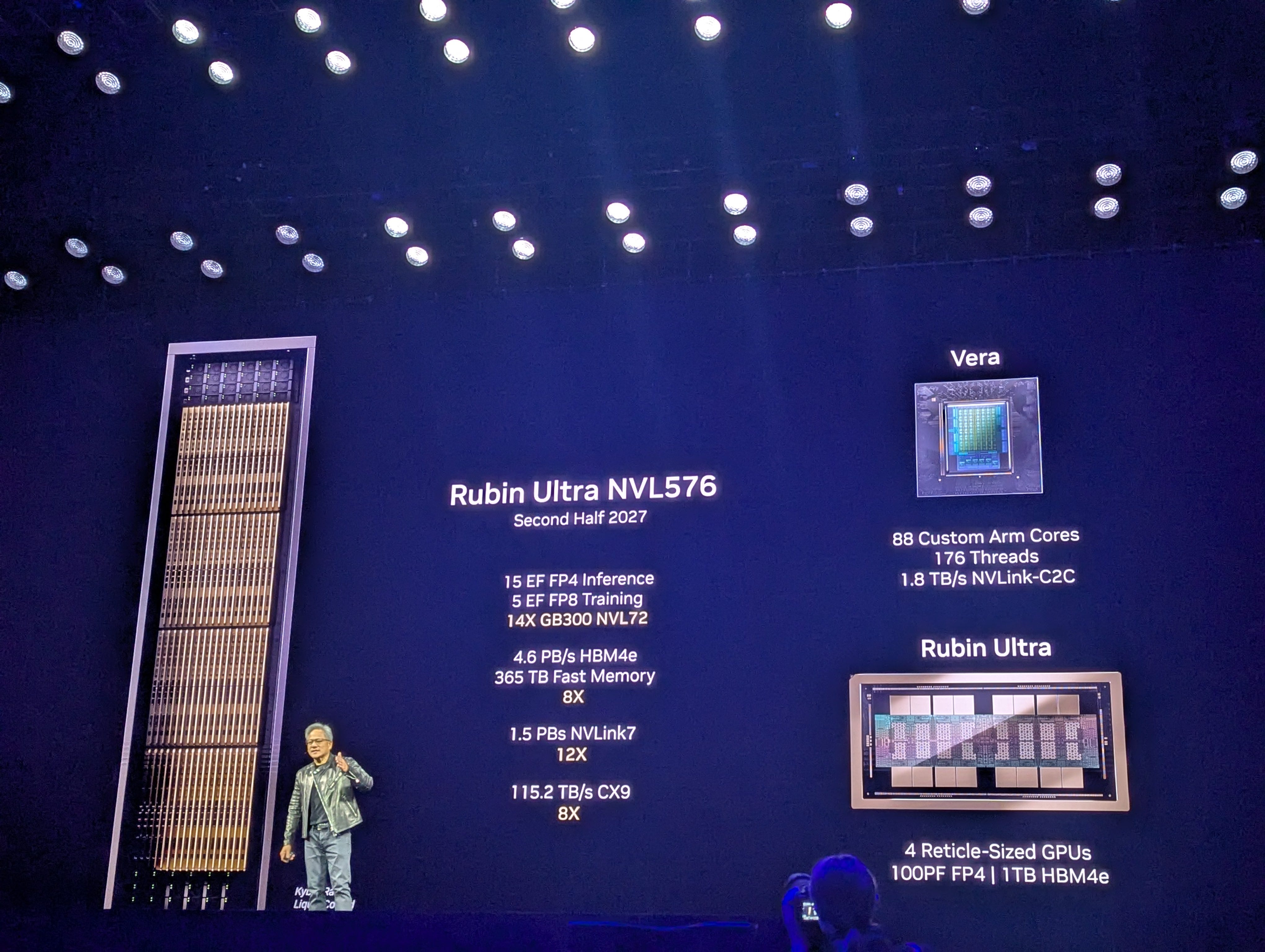
In the pursuit of density, Nvidia are planning to quadruple the GPU count in their rack-scale NVL SKUs for the peak of the Rubin generation, with the NVL576 consisting of 144 Rubin Ultra devices containing 4 reticle-sized GPUs each. For this, Nvidia are moving to an orthogonal blade server architecture for the racks, with the compute blades now being vertically slotted into a single tall chassis and with multiple such chassis in a rack. The NVLink switches will also be in blades but will enter from the rear of the rack and will connect to the GPU blades via multiple midplane PCBs which will sit between the compute and NVSwitch blades. Notably, the midplane will have no concessions made for airflow, as the entire rack – every GPU and CPU, every NVSwitch and PCIe switch, every memory module and SSD – will be liquid cooled, leaving room for a high NVLink socket density.
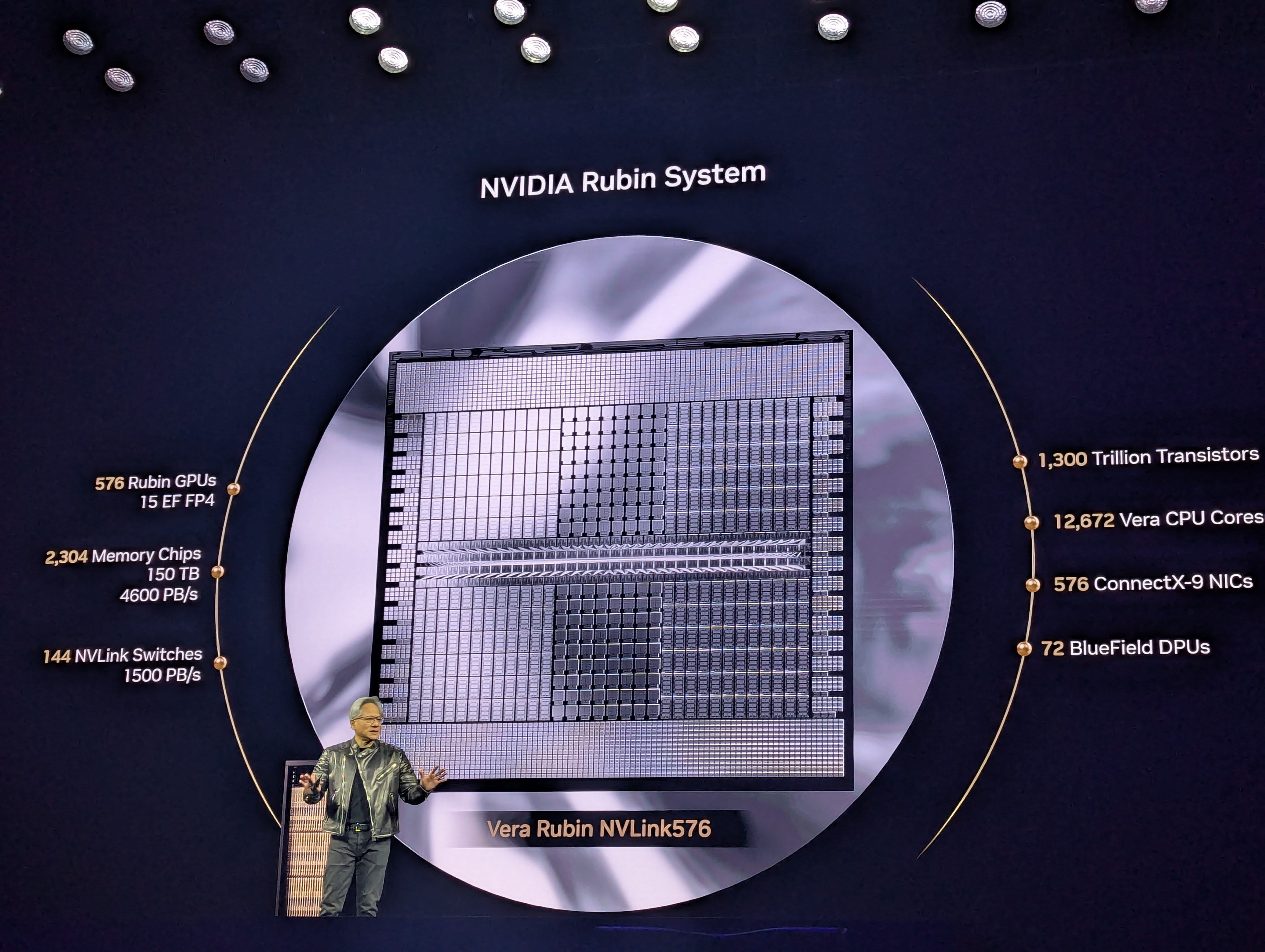
There are three points important of note for this architecture. Firstly, the count of 576 GPUs is due to Nvidia changing how GPUs are counted, with each chip being a GPU rather than each device being one. This means that conventionally, this rack would be known as an NVL288, though each of the chips will present as a GPU to the OS. Secondly, it’s unspecified yet how the 4 chassis in the rack will connect into one NVLink domain, or if the rack will present as a 4 x NVL144 instead of a NVL576, its possible Nvidia will still be dependent on DACs for this. Finally, whilst Nvidia claim the TDP is ~600kW, its possible the actual value may be as high as 819kW, as per SemiAnalysis’ prediction.
Finally, the specs (that we know of so far) (1 2 3 4 5 6):
288GB HBM4E per GPU, 4.6PB per rack
3.6TB/s bidirectional per GPU with NVLink 7
15EFLOPs at FP4, 5EFLOPs at FP8
288 CPUs w/ 88 Arm cores each, 25344 total
CX9 1.6T NICs, BF(4?) DPUs at 1.6T
365TB LPDDR(6?) system memory
1.8TB/s C2C between pairs of CPUs
TDP between 600kW and 820KW
Nvidia reveal plans for the GB300 NVL144 and HGX NVL16
Nvidia revealed their GB300 (Blackwell Ultra) rack-scale SKU as the NVL72 during Jensen Huang’s GTC 2025 keynote presentation, but with an emphasis on how a single chip will be two GPUs rather than one from now on. The new method of counting GPUs may take some time to propagate, but the availability of this SKU is practically imminent.
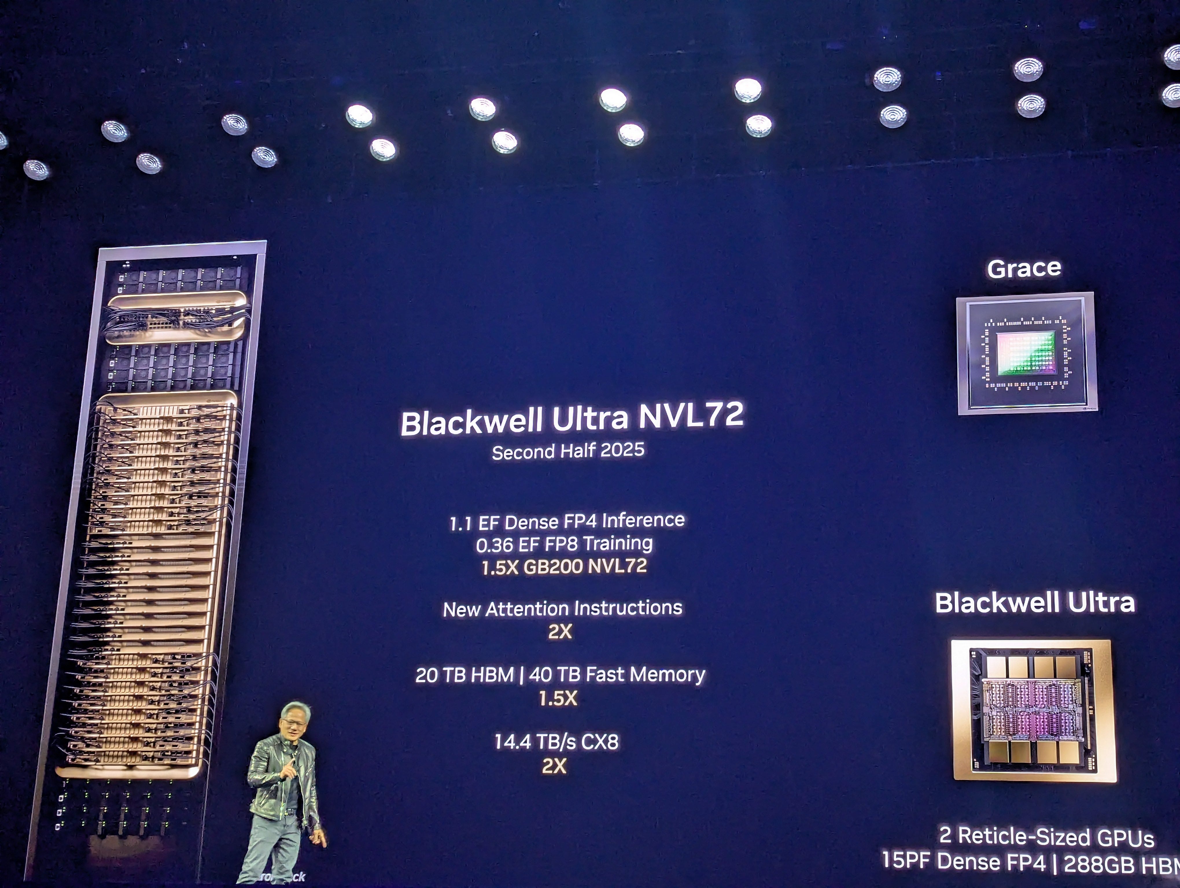
As expected, Nvidia announced the GB300 NVL72 rack-scale SKU, debuting the Blackwell “Ultra” GPU. This comes as a direct upgrade to the B200 with 50% greater FP4 FLOPs at the cost of almost all the FP64 capability, and an increase from 192 to 288GB of HBM3E. As for connectivity, the scale-up network will be NVLink gen. 5 providing 1.8TB/s bidirectional from GPU-GPU and the scale-out will use 800G CX-8 NICs with NDR800/XDR InfiniBand or 400/800G Ethernet. Though initially, only 800G InfiniBand deployments will be available due to release schedules for the SpectrumX switches supporting 1.6T ports.
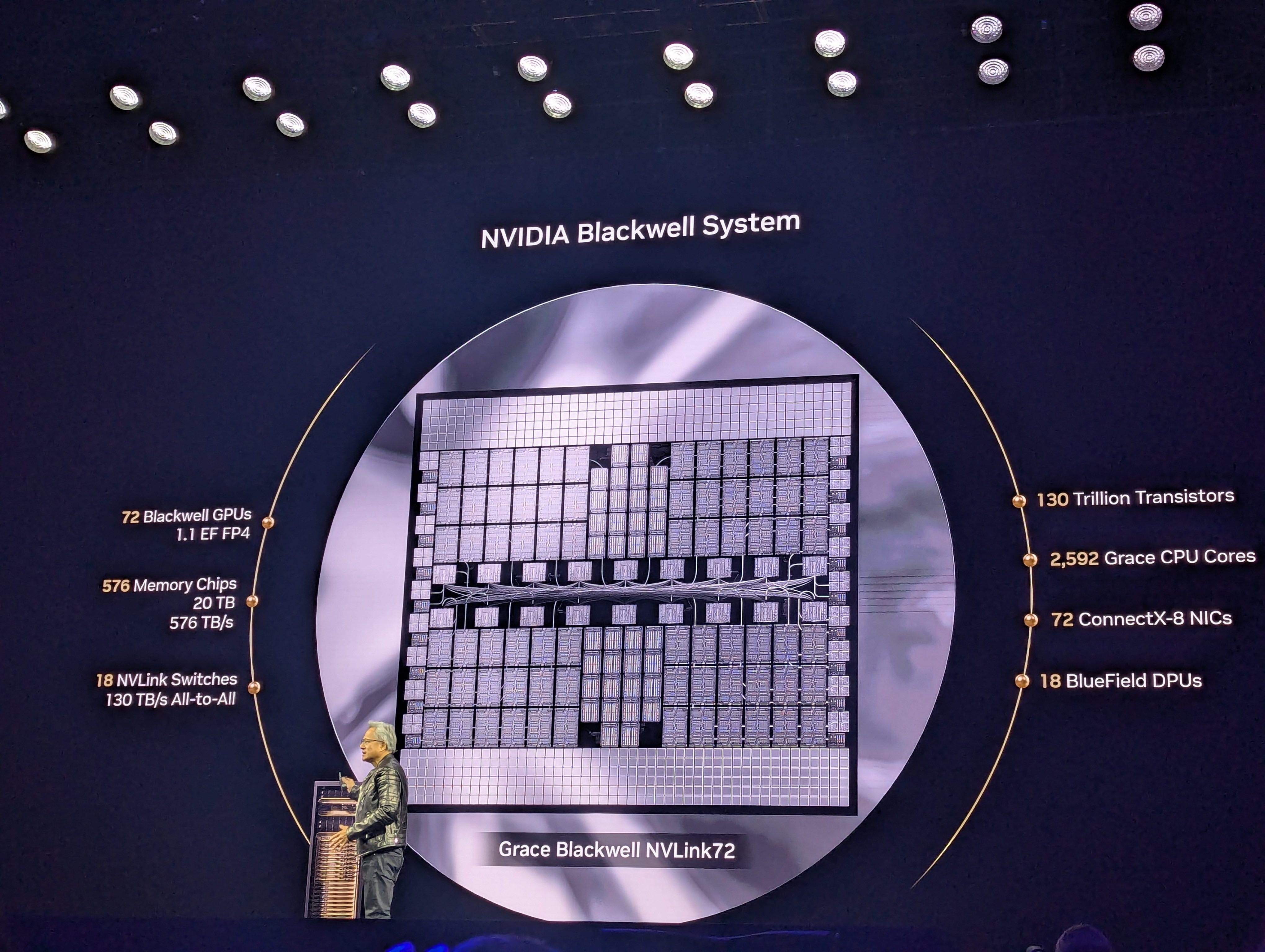
Vendors and integrators who are familiar with having to replace entire baseboards for GPU repairs and maintenance will now be able to provide better SLAs due to Nvidia putting GB300 devices onto easily replaceable sockets called “SXM pucks”. This is in line with the industry shift towards socketed, modularised solutions for high-power accelerators and memory devices. The GPU itself will still be a dual-die device which Nvidia have agreed for now to still refer to as a single GPU (at least for their NVL units), unlike in the HGX NVL16 which will be a single-die device with no high-bandwidth interconnect in between.
And of course, the specs, per GPU (1 2 3 4 5 6):
15/5/2.5 PFLOPs at FP4(dense)/FP16/TF32, ~1.4TFLOPs FP64 and 320TFLOPs INT8
288GB HBM3E, 8 stacks at 12hi (SK-Hynix exclusive), bandwidth remains at 8TB/s due to pin speed
CX-8 NICs, 1:1 GPU:NIC ratio, supporting NDR800/XDR and 800G Ethernet, with BF3 DPUs at 4:1
NVLink gen. 5 at 1.8TB/s bidirectional, using 224G SERDES across 36 lane-pairs (50GB/s each)
1.4kW TDP in GB NVL solution, 600W for the HGX version (per die)
Mixture of liquid and air-cooled variants available via vendors
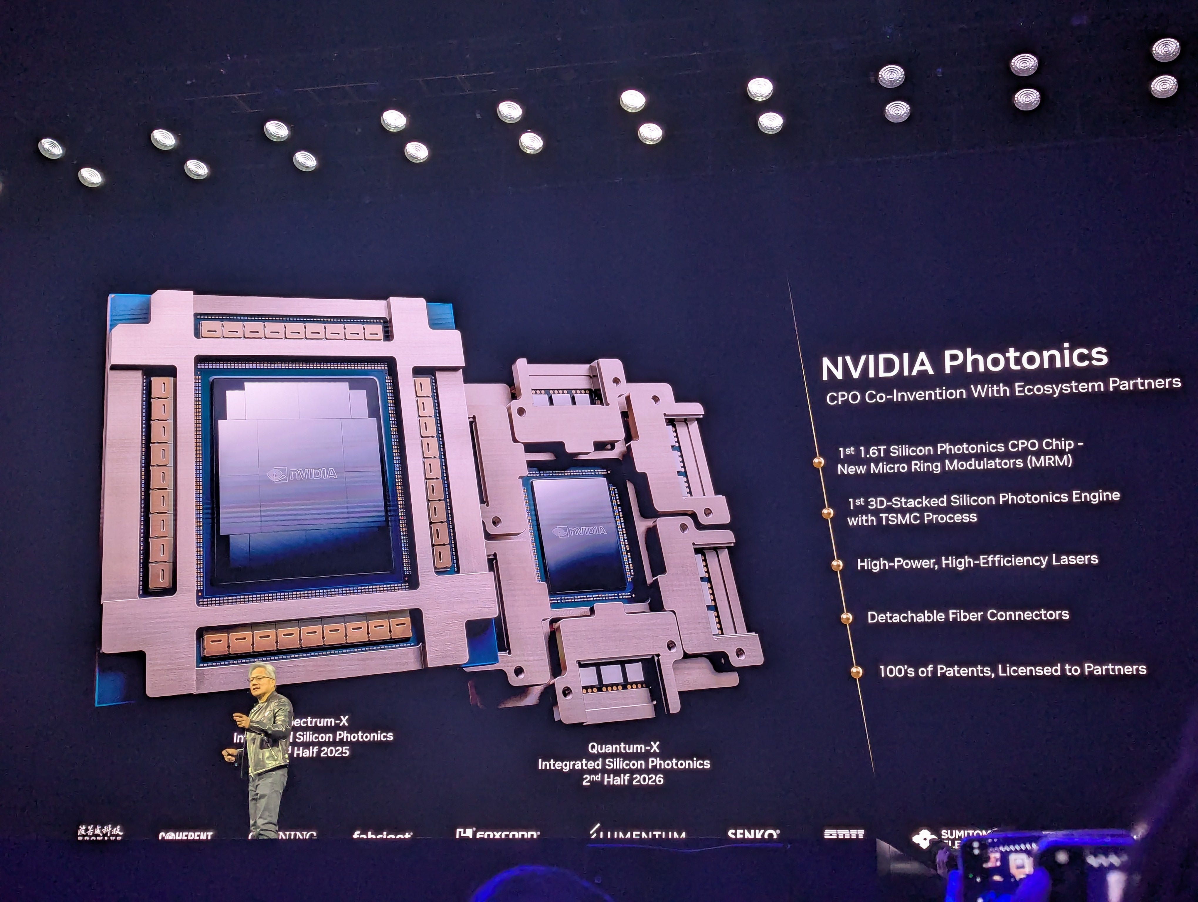
Nvidia and partners announce next-gen datacentre switches with co-packaged optics
The necessity of optical fibre in datacentres doesn’t imply the necessity of explicit optical-electrical interfaces, as TSMC and Nvidia demonstrate with their upcoming co-packaged optics switches. Their Quantum-X InfiniBand and Spectrum-X Ethernet switches, due for 2H2025 and 2H2026 respectively, aim to remove the need for optical transceivers entirely.
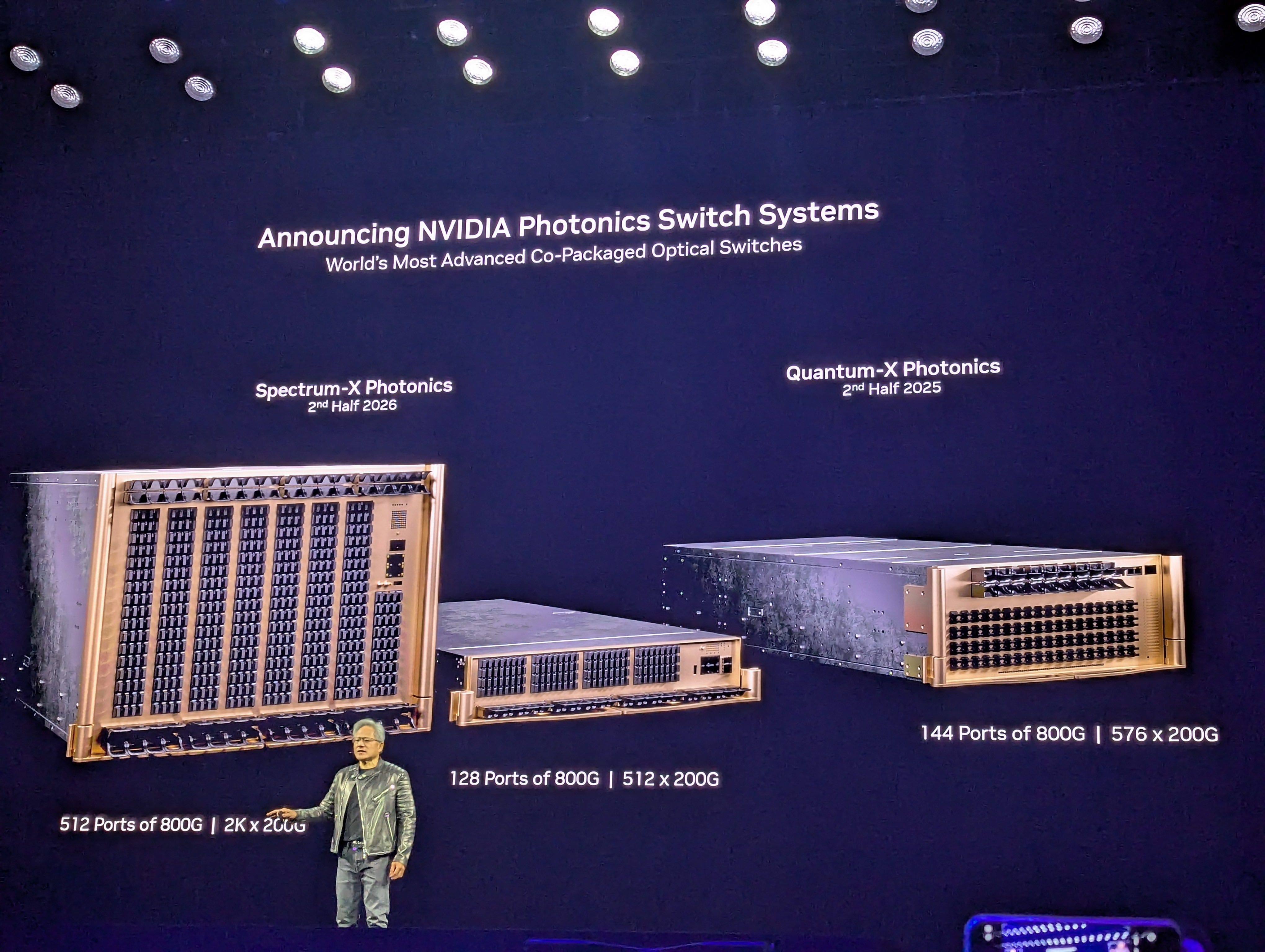
Anyone working in a datacentre will be familiar with the downtime caused by port-flapping, overheating, or just the eventual degradation of optical transceivers that servers and switches are increasingly requiring more and more of. At the GTC keynote presentation this year, Nvidia announced a collaboration with various industry partners on using co-packaged optics (CPO) to allow optical signals incoming from fibres to route to the ASIC package itself, rather than through a transceiver. Instead, CPO switches will use external laser sources to facilitate communication, which will come in similar form factors to SFP. Nvidia’s current roadmap includes a 144 x 800G QuantumX IB switch available in 2H25, and 128/512 x 800G SpectrumX Eth switches available 2H26.
Though not entirely avoiding pluggable, CPO switches still provide two key benefits to AI datacentres: significant power savings, and hardware volume reduction. Compared to electrical switches with optical/electrical conversions happening at each transceiver and then being propagated to the switch silicon, CPO switch ASICs now no longer need external digital signal processors for reducing noise and converting between digital and analogue signals. In addition to this, the switch interface itself can be much denser as optical fibres can plug directly into the switch, resulting in much higher port-counts and hence the ability to flatten the physical topology of a large network from three to two layers.
CPO technology will inevitably feature on NICs or even processor packages themselves, removing the need for transceivers on the server side too. As reported before in this publication and from industry rumours regarding future generations of Nvidia hardware, experimental CPO enabled designs for GPUs are already being developed for ~2027/28, hoping to allow fully optical connectivity from accelerator to switch.
Bolt Graphics reveals “Zeus” GPU – Claiming to 10x the Nvidia 5090’s performance
American startup Bolt Graphics claims that their upcoming Zeus GPU will provide 10x the graphics rendering performance of Nvidia’s flagship RTX 5090’s. But with up to 20 TFLOPS of FP64 and 2.25TB of memory per GPU all within a 500W TDP, the Zeus is sparking interest in both academia and industry for HPC workloads too.

Designed around enabling real-time model/graphics visualisation and handling larger frames than current rendering farms can handle, hardware design startup Bolt Graphics intends to accelerate intensive industrial graphics workloads with their upcoming Zeus GPU. In addition, early benchmarks show that the focus on supporting high-precision data formats also serves to accelerate highly-parallelisable scientific workloads such as electromagnetic wave simulations, with indicative performance being up to 300x that of Nvidia’s B200 GPUs. Initial samples are due in 2H25 and mass production is planned for 2H26, which places it two quarters ahead of Nvidia’s “Rubin” architecture-based RTX 60XX series according to our predictions.
Within a thermal profile of just 500W, the Zeus GPU provides 20 FP64 TFLOPs (vector) and 2.4 FP8 PFLOPs (matrix) to accelerate both high and low precision workloads, supported by 512MB of L2 cache, and a total device memory of 2.25TB - split between 256GB of LPDDR5X and 2TB of DDR on DIMMs - at 1.45TB/s. As for I/O, the device’s baseboard itself carries 6 OSFP 800GbE ports and 32 lanes of PCIe gen5 in total, allowing for a CPU-GPU bandwidth of up to 128GB/s and a GPU-GPU bandwidth of anywhere between 800-6400Gb/s (both unidirectional) depending on the data fabric topology. There are four variants of the Zeus planned currently: the single chip 1c, two variants of the dual chip 2c version, and the flagship 4c quad-chip version detailed above.
Most notably in their marketing material, Bolt Graphics claim that a single Zeus can replace 10 Nvidia RTX 5090’s in render farms, leading to a total power reduction of up to ~91% (based on a 5090 running at 575W). The primary arguments to support this statement likely centre on the new GPU’s significant FP64 support, large memory capacity, and incredible I/O bandwidth (which lends itself well to large rack-scale deployments), both of which the gaming-focused RTX-series GPUs lacks. The majority of this information is from the official slide deck here.
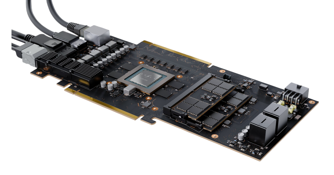
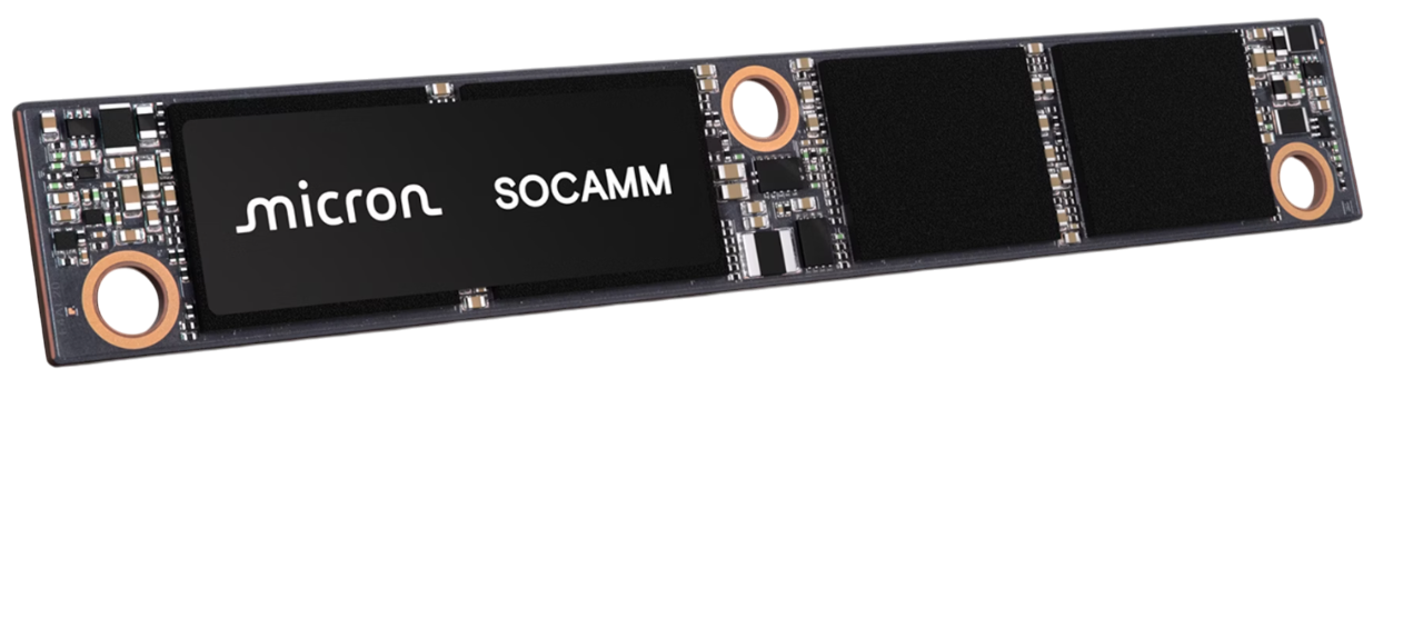
Micron secures first SOCAMM memory module supply for Nvidia GB300s
The market has been driven towards some fundamental changes in server PCB design in the past few years, one of them being the modularisation of various error-prone devices. SOCAMM, or the Small Outline Compression Attached Memory Module, is now quickly becoming the standard for replaceable, power-efficient memory on high-performing servers.
Conventionally, server memory is attached to the baseboard using DIMMs, which are designed to be easily replaceable in case of failure. This form factor does limit the performance of the memory though and so for high-bandwidth low-latency memory devices, soldering to the baseboard itself allows for the required performance without developing new module standards for each variation. Recently however, the industry has begun to move towards the SOCAMM design, allowing for a high-performance module that can be swapped out easily in case of device failure, avoiding requiring the entire baseboard to be replaced.
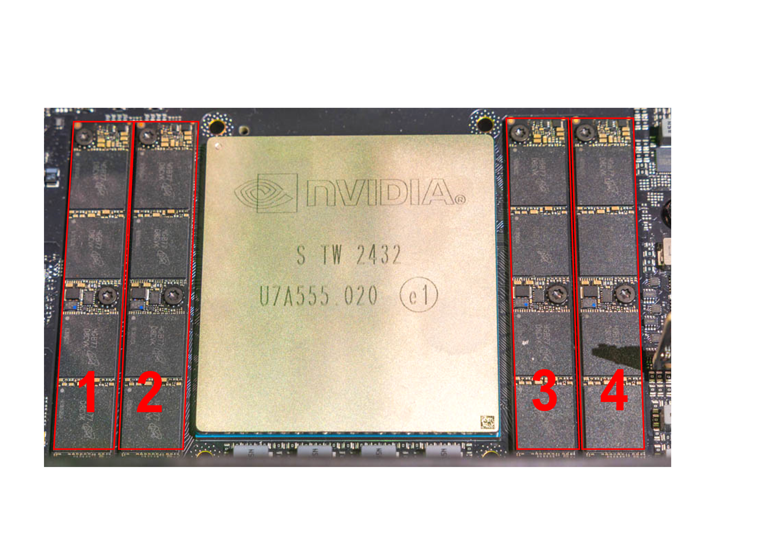
The Nvidia GB300 baseboards due in 2H25 will now include Micron’s SOCAMM modules for attaching up to 512GB of LPDDR5X to each Grace CPU on a 2 CPU + 4 GPU baseboard (codenamed the “Bianca” variant for the GB200s), with the CPU-memory aggregate bandwidth reportedly being ~400GB/s bidirectional, according to Nvidia’s official specs for the GB300 NVL72. This implies a distribution of ~100GB/s per module, each module including four stacks of 16 memory dies produced on Micron’s cutting edge 1b (beta) 10nm DRAM process. Micron state that their SOCAMM technology offers up to 2.5x the bandwidth of DIMMs in an equivalent capacity and configuration and reduces the power consumption by up to ~66%, though comparative benchmarks for GB300 superchips against GB200/GH200 variants (which used traditional soldered-on LPDDR5X) are not yet available.
Compared to the other two major memory manufacturers, Micron appear to be leading in DRAM process nodes as well as the overall power efficiency of their DRAM products, including HBM3E. Whether this lead persists into HBM4 is unclear as timelines between the three manufacturers for producing samples now differ by multiple quarters. SK-Hynix’s is reportedly still in the sampling process for their own modules, and Samsung are actively collaborating with Nvidia on prototyping this technology but have not announced any plans for their own SOCAMM products.
Other notable headlines
SK-Hynix ships first HBM4 samples to key customers, and reportedly secures exclusive supplier rights for 12hi HBM3E for Nvidia GB300s
Vendor spotlight:
Cerebras
In a semiconductor fabrication unit, the manufacturer partitions a large silicon wafer into lots of small chips and each of those then goes on to be integrated into a device such as a CPU or GPU. Cerebras instead decide that they will use the entire wafer and keep it in one piece, for an enormous, monolithic chip called the wafer-scale engine (WSE).
Conventionally, a chip designer would never consider using an entire silicon wafer as a single device, let alone exceeding the size limits of what can be fabricated without dropping yield rates. If a designer decides to pursue this regardless, then there are two significant issues to overcome: managing the impact of the inevitable manufacturing defects and designing the I/O software and hardware for connecting the wafer efficiently. Cerebras tackles both with their various innovative approaches and then packages their wafer-scale engine (WSE) in their “CS” systems.
Having defects during manufacturing that can cause a few cores to be written off are expected, and Cerebras works around these issues with its reconfigurable architecture that modifies the core-core interconnect paths dynamically around deactivated cores. In addition, connections between the die themselves are specially designed in collaboration with TSMC to enable cross scribe line communication, scribe lines being where the silicon is supposed to be physically cut. These technologies, along with many other advancements, enable the WSE to offer industry leading single-server specs.
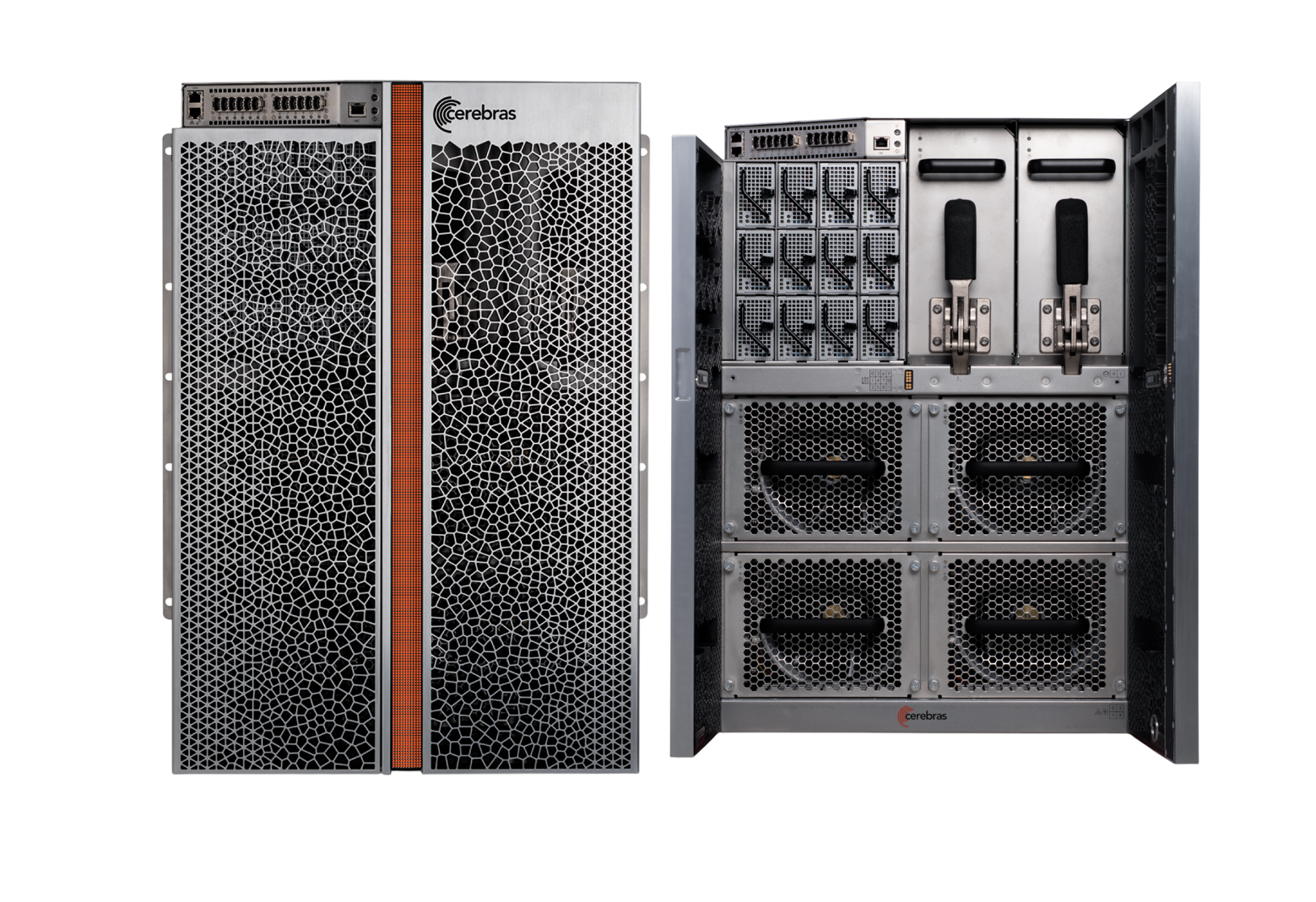
Here is what we know about the latest generation, the WSE-3 as revealed in 1Q24 (1 2 3 4):
A total of 125 PFLOPS of dense FP16 (most likely) at a TDP of ~23kW
44GB of “on-chip” SRAM, delivering an aggregate of 21PB/s of bandwidth from memory to the compute
214Pb/s aggregate bandwidth between all cores on the wafer using fabric routers and cross-scribe wires
Cerebras currently operate 3 datacentres with their 2nd and 3rd gen. CS-2 and CS-3 systems, and have confirmed an additional 6 across NA and EU by the end of 4Q25. Private sector customers include AstraZeneca, Total energies, Tokyo electron devices and more across NA and APAC. They also have significant presence in public sector research and academia, with Argonne, Livermore, and Sandia among the largest names in national labs currently confirmed to be trialling or purchasing CS-2 systems.
One-pagers:
Silicon binning
During the complex, multi-stage semiconductor manufacturing process, production errors can manifest in the final product as reduced clock rates, voltage instabilities, or even dead logic circuits. The process of sorting chips (that are intended to be identical) by their error rates results in a wide variety of functionalities and performances.
Semiconductor manufacturing processes - particularly for more advanced and performant process nodes such as what modern gaming and AI accelerators require - are prone to a large variety of errors such as contamination from dust, misalignment between various layers, or etching mistakes when shaping structures on silicon. Whilst these minor errors usually don’t write out the entire chip, they can manifest in a variety of issues which affect the performance of the final product due to requiring some sections to be deactivated and presenting as dead silicon. For example, a GPU that was designed to have 10 active cores at 1.5GHz could only have 8 at 1.4GHz after testing. Since chips are produced on large circular wafers, with up to 100s of chips on a single wafer, these errors can be distributed non-randomly across space resulting in distinct categories or bins that these chips can be put into based on how many defects they have.
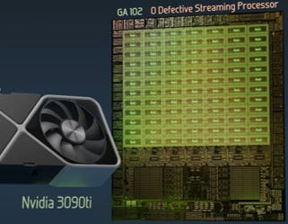
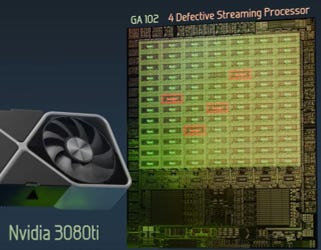
One outcome from this silicon binning process is that manufacturers can submit orders for the same chip design but then filter the end products into a variety of bins differing by performance to then sell them in various tiers. An example is Nvidia’s GA102/104 chips intended for their RTX 30XX gaming GPUs, with the lower end RTX 3080Ti and the higher end RTX 3090Ti sharing the same chip, but the former having an active core count of only 80 and a maximum boosted clock rate of 1.67GHz, compared to 84 and 1.86GHz for the latter. The differences in these values are great enough to lead to these nearly identical chips being packaged into two distinct products.
Even within bins, chip performance can vary greatly based on what manufacturers can’t or don’t control, such as clock rates, thermal performance differences, or transistor switching speeds. This results in a “silicon lottery” where despite buying the same equipment and providing identical running conditions, some end-users may report significantly higher performance from the same device, indicating that specifications provided by manufacturers may not be exact values but rather averages or minimums.
Branch prediction
Modern CPUs have been optimised to process multiple instructions simultaneously, billions of times per second, to allow for the performance that we expect. However, conditional instructions require choosing from diverging instruction streams which makes optimisation difficult. In these situations, CPUs employ specialised hardware for predicting the correct path.
To perform computations on data, hardware requires streams of instructions to inform it what to do with the data, and where to put the results. For most instructions, the result of the defined computation has no effect on the upcoming instruction stream, but in some cases the required instruction stream may change entirely depending on the result. This leads to the existing instruction stream and any intermediate computations already performed to be discarded and the processor state having to be traced back to when the instruction stream diverged or branched off.
For some instructions such as conditionals or returns, if the processor cannot anticipate the result of the computation before it’s complete, then it must either wait – wasting a lot of time and slowing down the task – or assume either outcome has a 50% chance of occurring and therefore choose one randomly to execute – Which could result in a misprediction, and a lot of time wasted again. CPUs solve this issue by using specialised hardware called branch predictors, designed solely to understand the instruction stream and predict where the stream might diverge to next, giving processors a higher probability of saving time for complex tasks.
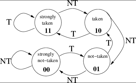
Structures such as 2-bit saturating counters as shown in the diagram are among the simplest of these predictors, where they flip between predicting that a branch should be taken or not taken depending on the counters state which changes based on how many times they have correctly or wrongly predicted the outcome. Moden CPUs use multiple and more complex predictors to make more informed decisions, with structures such as TAGE or neural predictors that consider the history of the instruction stream, its origin, and more to make informed predictions.