

June 2025
AMD charges full steam ahead, HBM might one day be more important than the compute, and Cornelis and Broadcom both innovate for datacentre networking

June 2025
This is the SixRackUnits AI hardware newsletter, keeping you up to date with the latest in AI hardware, datacentre technology, and the future of compute. In addition, we also cover vendors of anything interesting in the space, as well as short "one-pagers" on a random topic that we find interesting (and hope you do too).
For a space to share sources and news/updates, check out the notes section of this newsletter or my LinkedIn for posts on similar topics!
This month's updates:
AMD delivers a roadmap to defeat Nvidia
Broadcom shows the world a 100 Terabit switch ASIC: Tomahawk 6
1 PB/s planned for HBM within the next decade, KAIST reveals
OmniPath might still make a comeback: Cornelis announces the CN5000 spec
Other notable headlines
This month's updates:
AMD delivers a roadmap to defeat Nvidia
At their Advancing AI 2025 event this month, AMD delivered a reveal rivalling Nvidia's GTC last quarter. In it, AMD showed commitment to taking on the datacenter GPU market with a solid roadmap towards the most performant GPUs and the most ambitious rack-scale products planned for the next 3 years.
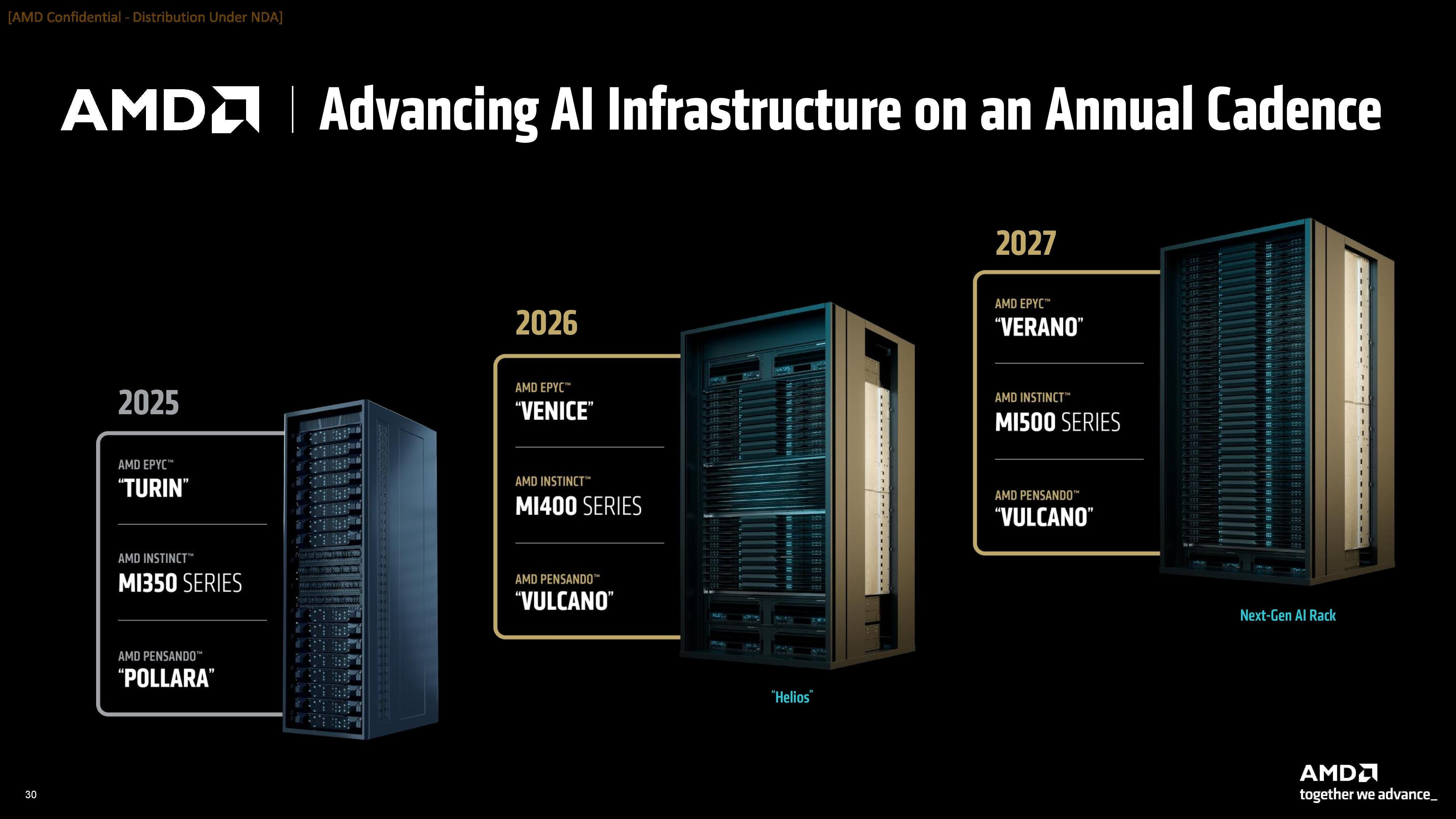
The roadmap charts a path through the three key routes towards dominance in AI training: CPUs, GPUs, and NICs. The Imminent "rack-scale" solution (2H25) is a not a particularly interesting stepping stone as it will still use a scale-out fabric between servers on the same rack, so as a quick summary: 64 MI350X air-cooled or 96/128 MI355X liquid-cooled GPUs, 5th gen. Turin CPUs, and Pollara 400G UEC (Ultra Ethernet Consortium) compatible NICs.
This product might still be quite popular among some hyperscalers wishing to deploy in volume, with OCI (Oracle Cloud Infrastructure) saying that they are preparing to deploy 130K (131,072) MI355X GPUs. This is unsurprising given that they have a very mature datacentre operations business and so won't be as impacted by the 40% increase in GPU TDP (see below for specs) as much as neoclouds or smaller datacentre build-outs would.
Given that there will be no APU form of the 350 series, it's entirely possible that the 355X was developed purely for Oracle and other hyperscalers who committed enough to justify a rather odd SKU like this.
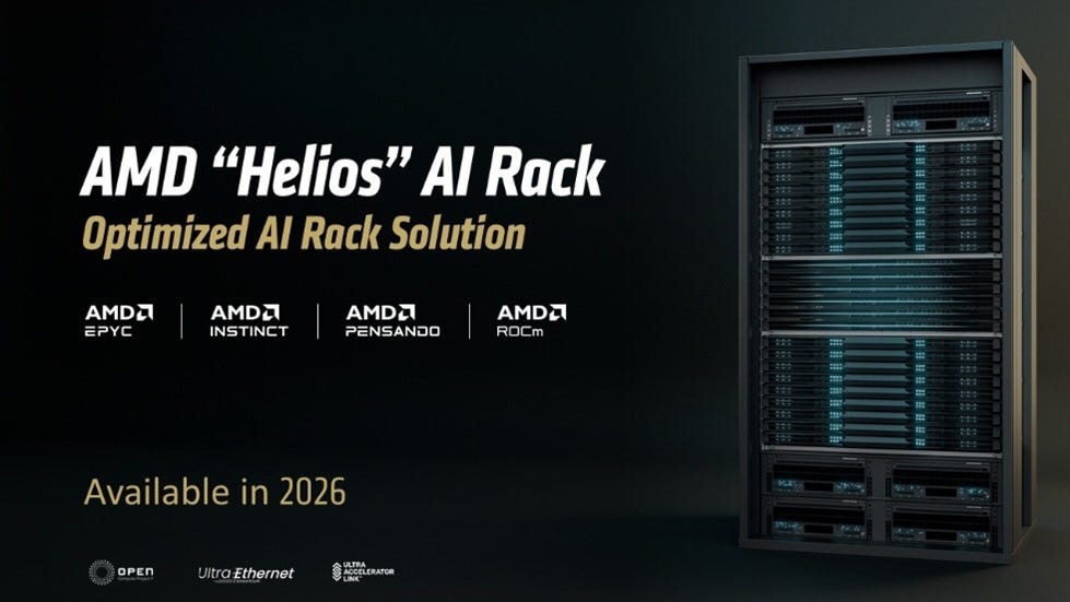
The much more interesting part of the future begins in 2H26 with what AMD call the "Helios" architecture. According to SemiAnalysis' estimates, this will be a double-width rack supporting:
72 MI400X or MI450X GPUs
18 7th Gen. "Venice" CPUs
216 "Vulcano" 800G NICs
6 scale-up trays @ 204.8T each
6 scale-out trays @ 51.2T each
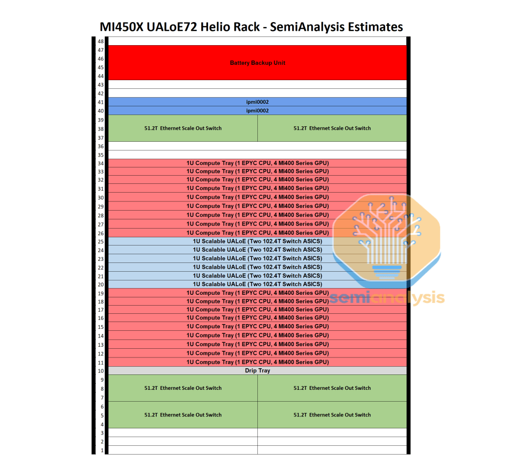
Below is SemiAnalysis' (estimated) diagram of the compute tray architecture:
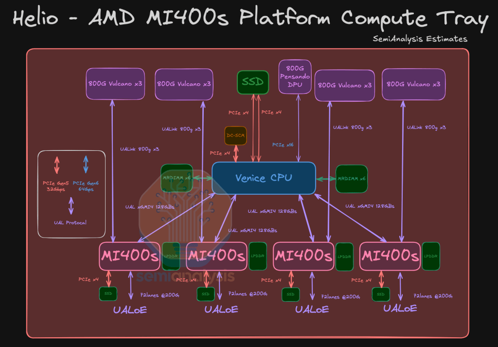
This implies the following specs:
720 PFLOPs at FP16
31.1 TB/s of HBM4 @ 1.4 PB/s aggregate bandwidth
~130 TB/s all-all scale-up bandwidth
~173 Tb/s (bits, not bytes) uni-directional aggregate scale-out bandwidth
These values are designed to match/surpass not Nvidia's Blackwell Ultra (GB300), but the Rubin's (VR200) expected performance. In terms of scale-up domain, AMD is targeting NVLink gen. 5 (1.8TB/s), and for the scale-out they're pushing past at 2.4Tbps/GPU, 1.5x that of NVidia's plans built around its upcoming CX-9 NICs.
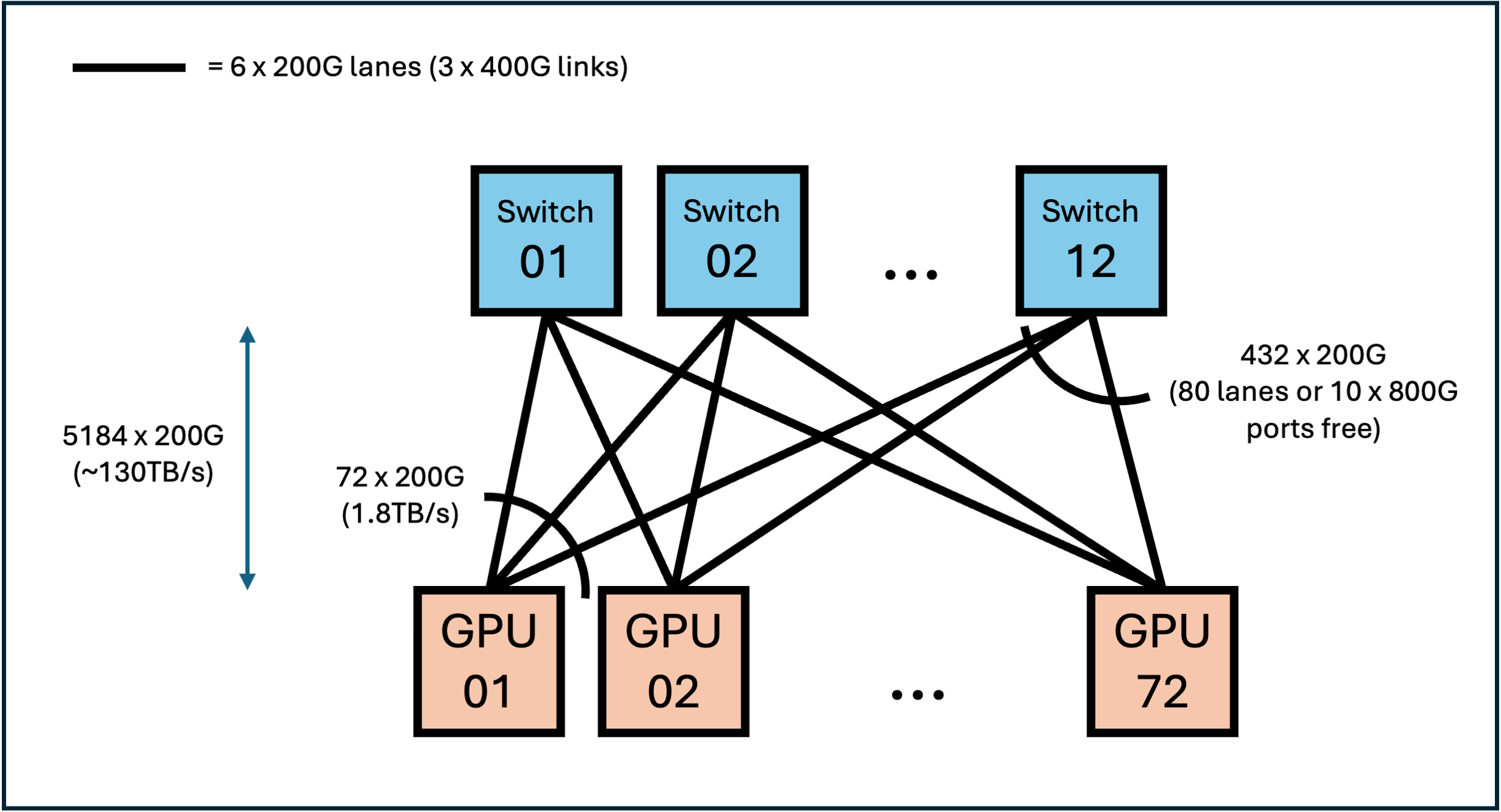
The options available for the topologies here are quite interesting. If we assume the SemiAnalysis estimates for the Helios's architecture, then the scale-up will be powered by 12 x 102.4T ASCIs (Broadcom's Tomahawk 6 is the only one available currently) which will present as 512 x 200Gbps ports each, for a total of 6144 x 200Gbps or 85.3 x 1.8TB/s connections. This means that each of the 12 ASICs can take 432 links, 6 from each of the 72 GPUs, and each GPU in turn exposes 72 links to the network. One possible topology is shown below:
Similarly for the scale-out, one possible simple topology is given below:
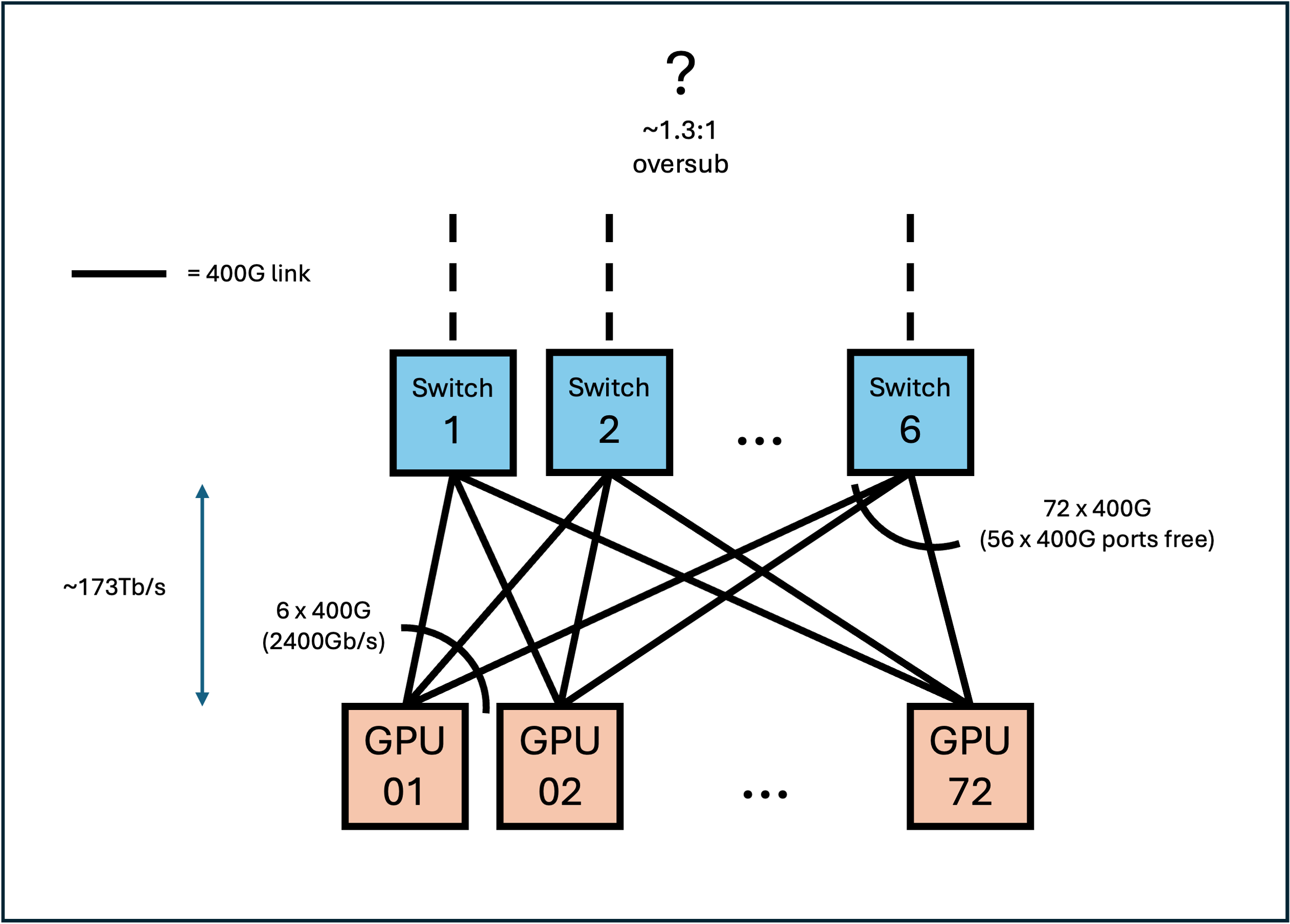
In both cases, we assume that the Vulcano 800G NICs would present dual 400G ports each, which would have the primary benefit of allowing for a wider range of OSFP or QSFP/QSFP-DD optics rather than 800G OSFP or other niche form factors albeit at the cost of additional parts and perhaps more energy consumption. In the case that NICs adopt CPO (Co-Packaged Optics) technology (though there isn't any information on this), then optics wouldn't be a factor but multiple ports would still be better in terms of redundancy and perhaps even performance.
Speculation: It's possible, but not supported by any sources yet, that AMD could move towards a dual (or even triple) plane architecture such as Alibaba's HPN. In this design, two identical versions of a 400G network connect to the same endpoints providing additional paths and hence more options for the network management algorithms to keep performance high under heavy, chaotic traffic patterns. In this case, it could mean that that each scale-out switch contains two 25.6T switch ASICs for physical separation of the planes, or that only three or two of the 6 switches are used per plane. Diagrams not provided.
Finally, some stats for all the new reveals, including both confirmed and estimated values (1 2 3 4 5 6):
MI350X:
288GB HBM3E 12Hi @ 8TB/s: 8 stacks of 36GB each (Samsung + Micron)
~4.6/9.3/18.5 PFLOPs @ FP16/8/4, ~72/144 TFLOPs @ FP64/32
1000W TBP (Total Board Power)
Using TSMCs "N3P" 3nm and "N6" 6nm processes
Shipping 2H25
256MB AMD "Ininifity Cache" (sort of similar to L3 cache)
PCIe 5.0 x16 H2D interconnect
1/2.2 GHz Base/Boost clock
Focusing on air-cooled deployments
MI355X:
288GB HBM3E 12Hi @ 8TB/s: 8 stacks of 36GB each (Samsung + Micron)
~5.0/10.1/20.1 PFLOPs @ FP16/8/4, ~79/158 TFLOPs @ FP64
1400W TBP (Total Board Power)
Using TSMCs "N3P" 3nm and "N6" 6nm processes
Shipping 2H25
256MB AMD "Ininifity Cache" (sort of similar to L3 cache)*
PCIe 5.0 x16 H2D interconnect*
1/2.4 GHz Base/Boost clock
Focusing on liquid cooled deployments
MI400X:
432GB HBM4 @ 19.6TB/s:
~10/20/40 PFLOPs @ FP16/8/4
2300W TDP
1.8TB/s scale-up bandwidth
2400Gb/s scale out bandwidth (3 x 800G NICs per GPU)
MI450X:
Nothing new of significance found yet
MI500X:
Reportedly either TSMCs "N2P" 2nm process or some 14A process**
*Assuming that the 355 will be very similar to the 350 in terms of architecture and composition. **The source that claims that the MI500X will use a 14A process node does not provide any justification for this statement.
SemiAnalysis and other sources mentioned above go much further into the details of the announcements, they are all well worth a read.
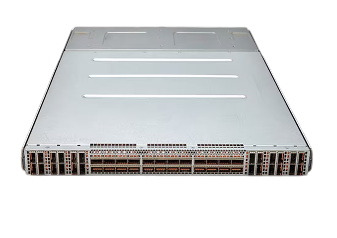
Broadcom shows the world a 100 Terabit switch ASIC: Tomahawk 6
51.2T switches - network switches that support up to 51.2 Tbps of aggregate bandwidth - are still only seen in large-scale high-end AI datacentres. Usually implemented as a 2U chassis of 64 x 800G ports, these switches power modern non-blocking east-west or backend fabrics. With the cable densities and transceiver counts used in large scale deployments such as Nvidia SuperPods, many datacentres have had a difficult time adapting to such high-bandwidth networking infrastructure.
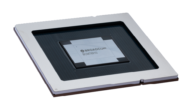
Despite all of this, Broadcom targets the prepared and eager datacentres of the near future by announcing a 102.4T switch ASIC: the Tomahawk 6. The chip will come in 512 x 200G lane and 1024 x 100G lane SKUs, with the latter being significantly larger due to the increased shoreline (perimeter) required to support that many physical lanes. In addition, a CPO (Co-Packaged Optics) version of the chip will be available, for near-future switch platforms competing with Nvidia's upcoming QuantumX-800 and SpectrumX products.
Note that this is not a 102.4T switch, which may consist of multiple ASICs (chips), but a single chip.
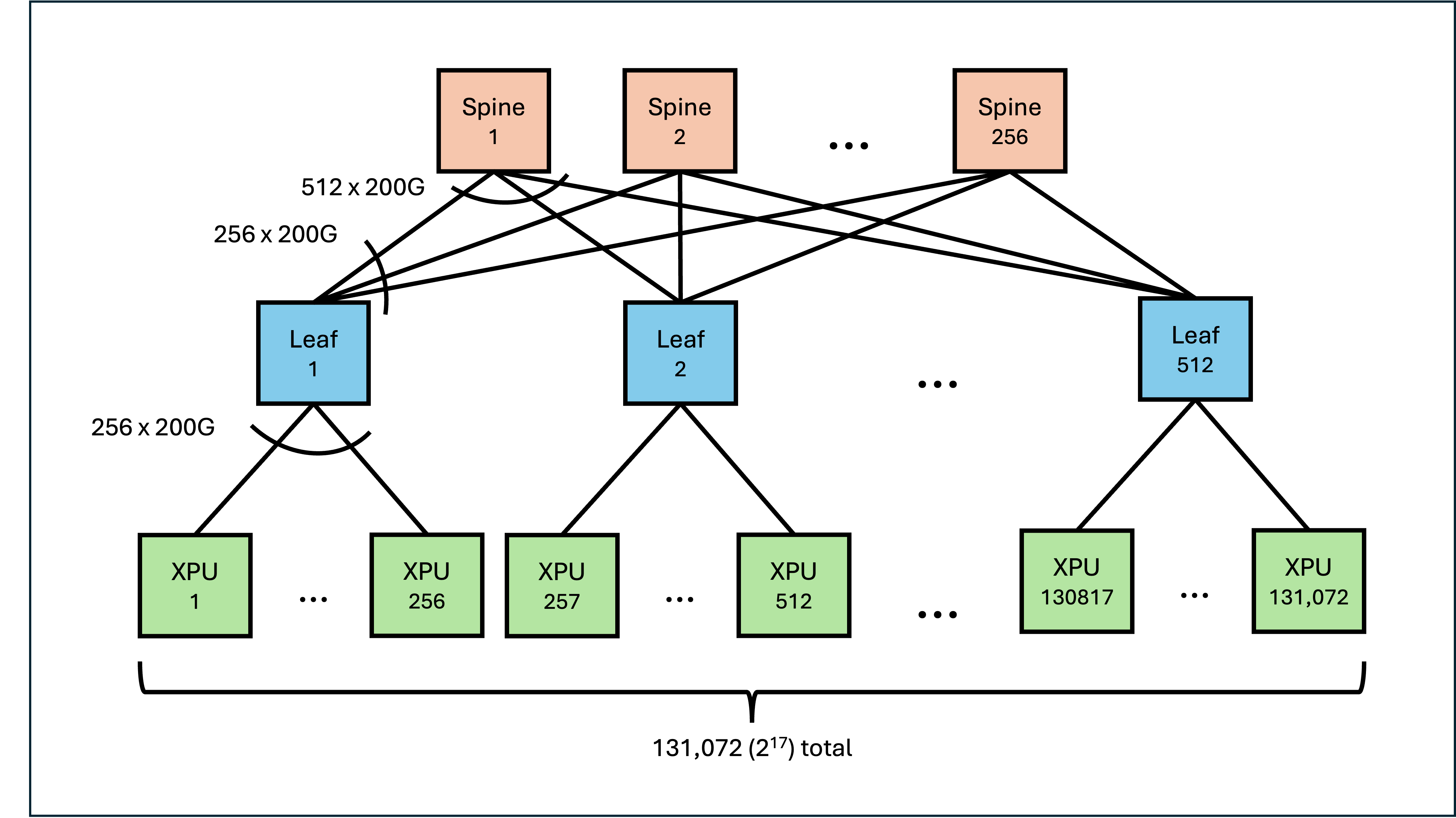
Among the many claims made by Broadcom regarding the ASIC's performance, the most interesting was its ability to support 100,000+ "XPUs", or devices, on a two-tier network. Typically, for a non-blocking spine-leaf network topology as is common in Nvidia's SuperPod reference architectures, three tiers of switches are required when scaling to large numbers of devices. This is because in switches like Nvidia's SN5600 and Arista's 7060DX5-64S provide 64 ports of 400G each, which means that a single switch can connect to 32 devices at 400G (the other 32 ports are needed for uplink to the spine layer). With this domain size for a single switch, 64 such switches can be used in the leaf layer, with each spine switch having 64 ports to connect to each leaf switch. This then implies a maximum of 64 x 32 = 2048 devices in a two tier topology, using these switches, at a 400G bandwidth.
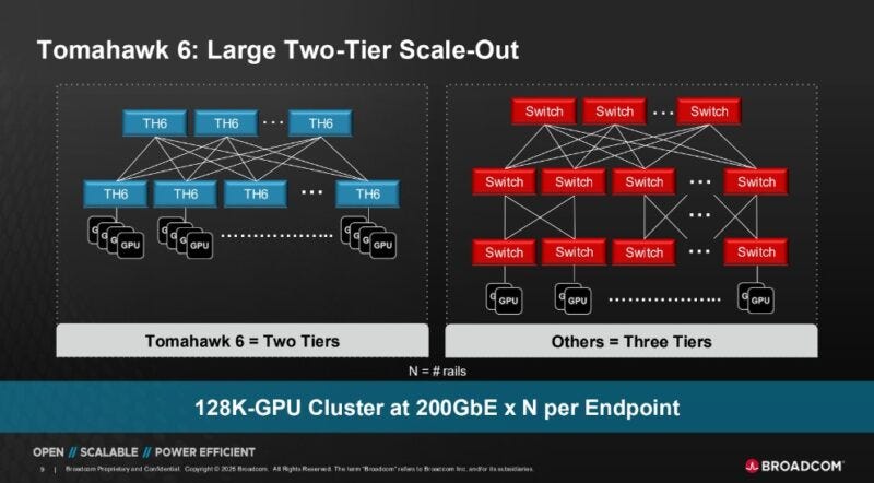
The Tomahawk 6, on the other hand, is promised by Broadcom to support 131,072 devices at 200G. One possible topology is shown below, a non-blocking spine-leaf setup (not-rail optimised because the diagram would get too complicated). To increase the bandwidth of the fabric without introducing a third tier, multiple "planes", or parallel implementations of this topology, can be used with extensive breakout in the ports/cabling. The benefit of such a setup would be the simplicity retained by each two-tier plane when it comes to congestion control, resulting in a more efficient and performant fabric overall.
The customers for the ASIC haven't been made public yet, but it's confirmed that sampling is underway, with mass production and hence integration into switches expected to start in 2Q26.
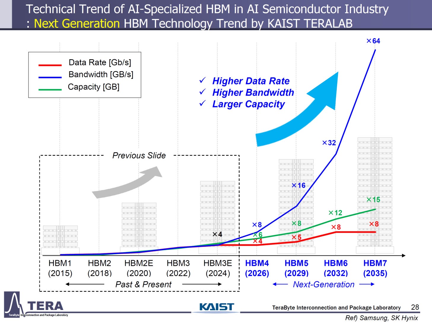
1 PB/s planned for HBM within the next decade, KAIST reveals
The 3 major memory makers - SK Hynix, Samsung, and Micron - are all working on HBM4 implementations, hoping to secure orders from the likes of Nvidia and AMD for their upcoming GPUs. The balance is tipping it seems with SK-hynix already sampling HBM4 and possibly even discussing custom HBM4 implementations with some customers, whilst Samsung is still struggling to pass Nvidia's qualification for HBM3E, but there is still a lot of potential for change.
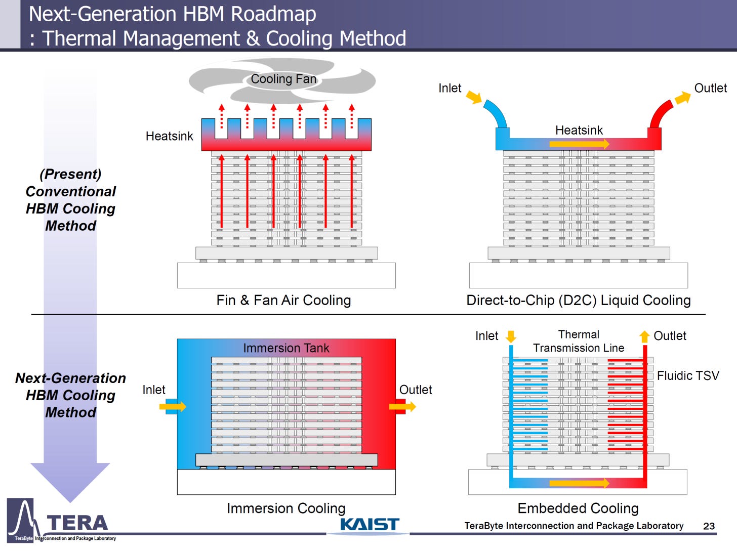
Meanwhile, the Korea Advanced Institute of Science and Technology, or KAIST, Teralab research group recently presented a roadmap detailing the current trends and future plans for HBM. Extending out to 2038, the roadmap reaches HBM8 and speculates that packages (device chips) will reach ~1PB/s of aggregate memory bandwidth from 6TB worth of HBM modules, as well as requiring up to 15kW of power and futuristic "embedded-in-chip" liquid cooling methods.
Teralab have an extensive history of research on semiconductor packaging, interconnects, and HBM in particular, and have also collaborated with both SK Hynix and Samsung on HBM and surrounding technologies. The 371-slide presentation was part of a significant effort to understand the current technological and economic trends shown in the memory markets in addition to well-informed speculation based on current and planned research. The full slides are available here.
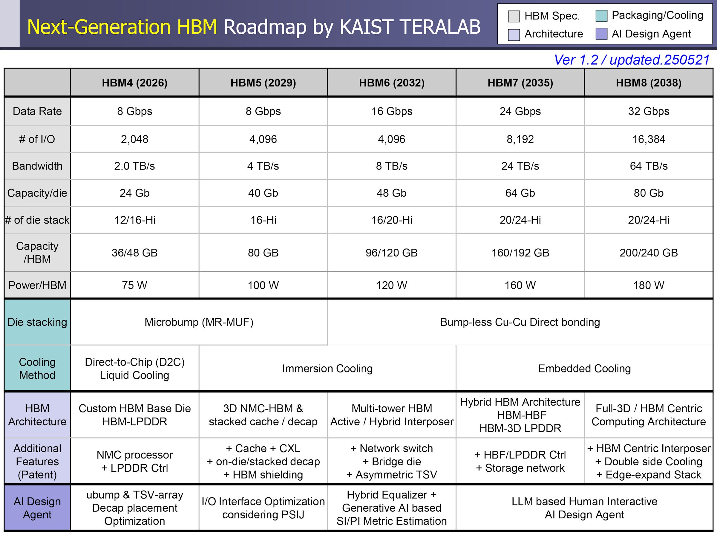
According to forecasts by the group, data rates for pins that connect the HBM module interface to the compute dies will level off at about double that of current HBM3E implementations. The capacity of individual memory dies however, should increase by ~3.5x, driven by denser process nodes and large die sizes. The leading hope for these incredible predictions though is the total module bandwidth increase, expected to jump sharply over the next decade due to stack height and bus width increases.
Based on how the increased stack heights, die densities, and module power usage all compound to increase heat generation, current cooling methods will not be able to keep up. Teralab propose two new methods: dedicated module immersion tanks and in-chip embedded liquid cooling.
The former is implemented already at a more macro-level, where entire servers can be dipped into tanks of non-conductive fluids, but is still constrained to research lab supercomputers (1 2) rather than hyperscaler datacentres. The proposed method here however shrinks the domain of immersion to the chip/stacks themselves, isolating the fluid but also allowing for a dedicated fluid supply to each module.
The latter is seemingly a much more complex and involved method requiring integrating the cooling system into the chip manufacturing process too, but appears to show promise for significantly cooling capabilities than current industry conventions. Presently, implementations of all such cooling systems remain in the research domain (1 2 3).
The presentation goes further into specifics on current and future research streams, and also talks about future SoC (System-on-Chip) designs created around HBM stacks rather than compute chips. Detail is given on how other memory technologies such as LPDDR die and HBF (High Bandwidth Flash) can be integrated onto future packages, controlled by HBM logic die to provide CPU-independent tiered memory systems for compute. For more on this, see the slides here.
OmniPath might still make a comeback: Cornelis announces the CN5000 spec
The modern networking market for AI is often seen as a two-horse race between InfiniBand and Ethernet, the first being an established standard for HPC and AI applications, and the second being the underdog who is rapidly catching up at smaller and medium scales and usually was the only real solution at extremely large scales. But there are other players each bringing their own pros and cons, but most only really being useful in very specific situations.
OmniPath, now advanced by Cornelis networks (but developed originally by Intel), is another competitor which appears to meet the criteria for being a viable datacentre data fabric: scalability, performance, and availability.
Introducing speeds of up to 400Gbps for a lossless and congestion-free fabric, as well as message injection rates "2x greater than InfiniBand NDR", OmniPath is sticking to its USP of having better latency. Though now, rather than staying in the shadows with research labs running HPC applications, Cornelis wants to bring OmniPath into the limelight with AI.
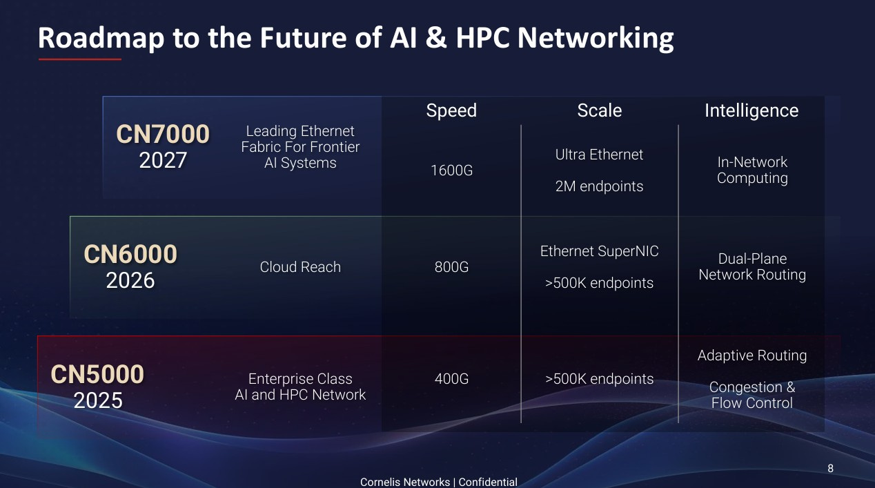
This is essentially the same plan they had in 2024 as well, predicting that UEC (Ultra Ethernet Consortium) compatible hardware would only be available in mass around 2027, despite the standard being finalised just this month. This is a sensible bet given how long it takes consortiums to progress from paperwork to implementation but given the urgency that industry is showing when moving away from InfiniBand, its possible that vendors will release limited ranges ofUEC-ready products in 2H25
Current plans for the CN5000 technology is to support 400G fabrics for up to 500K endpoints (devices), but by 2027 that should quadruple to 1.6T and 2 million endpoints, showing a good understanding of where the market is heading for hyperscalers, neoclouds, and AI labs. In addition, OmniPath will support Ethernet next year and then UEC the year after next, signalling that Cornelis do not intend to make the same mistakes that Nvidia did until last year with aggressive vendor lock-in through InfiniBand.
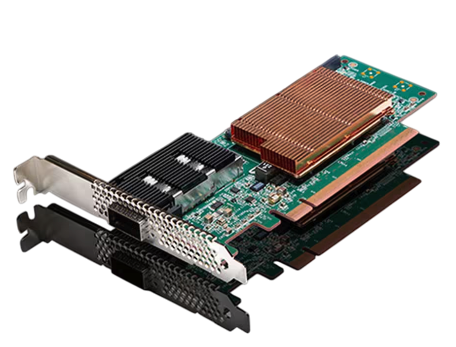
The CN5000 SuperNIC comes in single or dual port PCIe form factors, using gen 5. (~64GB/s uni-directional). Cornelis state the power draw to be 15 or 19W for the single and dual port versions, and will provide SKUs for air-cooled and liquid-cooled versions. One source claims that the NIC is capable of 800 million packets per second, and provides "<1 microsecond latency for MPI" though there are no other sources to corroborate this.
The switch is a 1U, 48-port chassis, with a TDP of 710W empty, or 1.1kW with 48 7.5W AOC (Active Optical Cables) ports. 48 ports is an odd number, and might be from some combination of having multiple interconnected ASICs inside, keeping the form-factor to 1U, reducing or managing latency by keeping the port count low, or some other optimisations to the ASIC for the incredible message rates OmniPath provides. These switches will also come in air and liquid-cooled SKUs.
It should be remarked that very few vendors are open about the power draws of their switches and NICs publicly like Cornelis is.
Other notable headlines
Chinese-aimed RTX Pro 6000D may well have NVLink after all, analysts suggest
PCIe 7.0 official specification is live, despite gen. 6 adoption being barely visible in industry
Samsung yet again fails HBM3E certification on Nvidia packages, aiming for a re-run in September
AMD's Zen 6 architecture could lead to 7 GHz boost clock rates on CPUs