

August 2025
HotChips 2025 edition! Broadcom can't stop releasing switch ASICs, and PCIe 8.0 announced.

August 2025

Is a material form a requirement for true intelligence? Does being limited to certain modalities of input result in less capability within those modalities than an intelligence that can handle more modalities of input? If so, will achieving human-level intelligence require AI models to have humanoid robotic bodies?
This is the SixRackUnits AI hardware newsletter, keeping you up to date with the latest in AI hardware, datacentre technology, and the future of compute. With a field changing this fast, staying on top of everything, or even summarising all the material available can be difficult - so we do it for you.
For a space to share sources and news/updates, join our telegram channel here or if you like short form posts on similar topics, check out the notes section of this newsletter or my LinkedIn.
This month's updates:
HotChips 25! - everything of note
Yet another switch from Broadcom - scaling across with Jericho4
B300 GPU finally detailed
PCIe 8.0 announced
Other notable headlines
This month's updates
HotChips 25! - everything of note
HotChips is the annual industry event for high-performance silicon, with both the big and small names showcasing their advancements in the field. This year's event seemed dominated by relatively few players, Nvidia, Meta, and Google stealing much of the spotlight. Between all the announcements and reveals made at the event, there were just too many updates to cover here comprehensively. Instead, we'll present some of the highlights that we think are the most important and interesting.
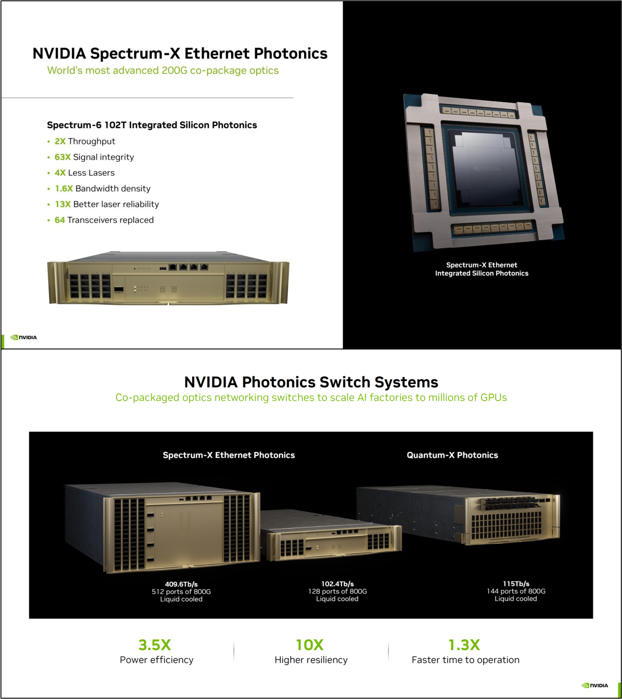
Nvidia: Spectrum-X switches and a scale-across fabric
Spectrum-X was originally Nvidia's reaction to Ethernet gaining traction after the market showed strong signs of InfiniBand lock-in fatigue. Now, rivalling InfiniBand in its adoption among Nvidia's largest customers, Spectrum-X is innovating in two key areas: massive 512-port 400T switches, and expanding beyond the confines of a datacentre.
Source: Nvidia
On the first item, a lot was already revealed back in GTC25 in March, see our article from back then detailing almost exactly the same information. The only new content is some more detail on the observed (we assume) performance (according to Nvidia) of the 102T switch, and pictures of the switch that uses optical transceivers rather than the CPO version that was shown back then.
Source: Nvidia
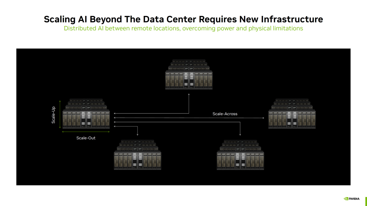
The other major reveal was the Spectrum-XGS add-on to Nvidia's ethernet fabric technology, a "scale-across" stack designed to connect multiple scale-out domains (datacentres) together. More on the meaning of scale-across in our article later in this post. Spectrum-XGS claims to expand telemetry, congestion control, and load-balancing all indefinitely with respect to the number of devices, and should be a lot better at reducing cross-datacentre latency where connections can be an order of magnitude or two longer than those within a datacentre.
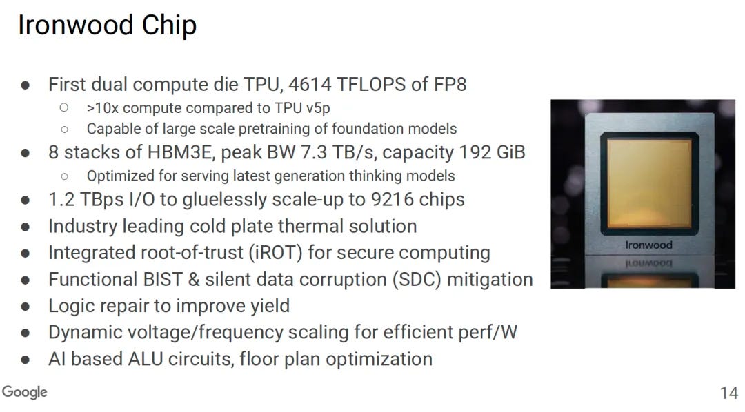
Google: Ironwood TPUv7 and TPU racks
We shared everything that was available on the TPUv7 back in April when it was announced, and a lot of this remain unchanged. We made a mistake in thinking it would be six stacks of 12hi HBM3E, and we now see it'll be eight stacks instead. Memory capacity and bandwidth remain unchanged thankfully. The compute capacity is interesting though, since at 4.5 PFLOPs of FP8, the TPUv7 brings the same amount of inference performance as the B200/300 and the MI350X. It seems the TDP hasn't yet been confirmed but anything below 1kW would be surprising.
Source: Google
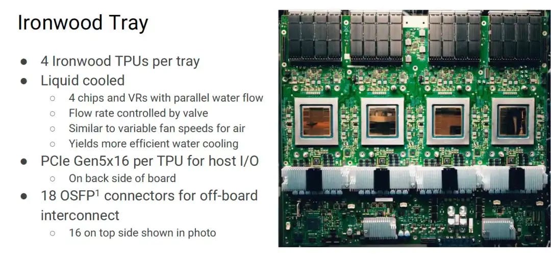
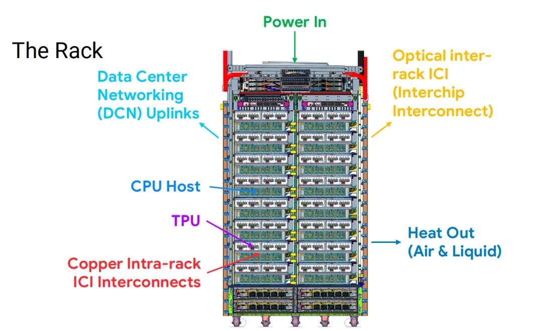
But Google's session was still very revealing, as they showed much more on how the Ironwood scales to the server and rack level. We saw earlier that they were aiming for 4 chips per board, but now its been confirmed in their slides. They're sticking to PCIe 5.0 for the H2D, which is unsurprising given that TPUs rely entirely on their mesh scale-up for D2D. For this purpose, they'll have an incredible 18 OSFP (800G) ports per board, so many ports actually, that they couldn't even fit all 18 on one side of the board and instead had to put 2 underneath on the other side.
It was also really interesting to hear them talk about the per-chip variable flow rates for the liquid cooling step. Having a constant and equal flow rate was just assumed to be the sensible idea, but different chips on the same board could be doing very different things in theory, and hence will need different coolant flow rates.
Source: Google
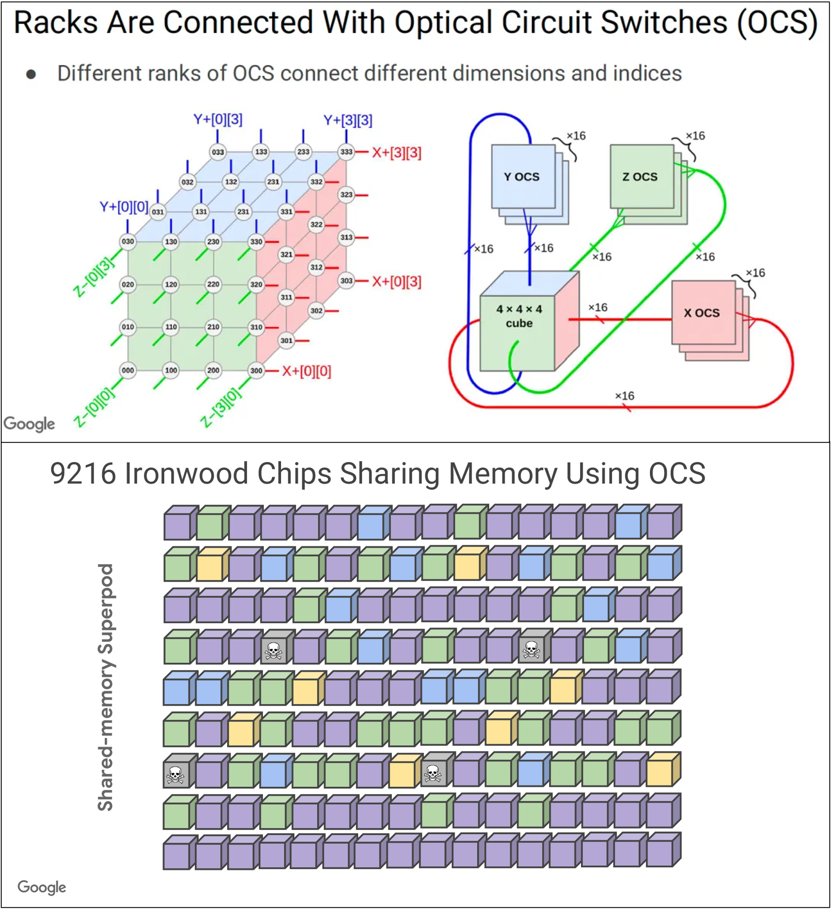
We knew they'd be aiming for clusters (or "pods") of up to 9216 devices in a single ICI (Inter-Chip-Interconnect) domain and predicted two topologies: a 96x96 2D torus, or a 32x32x9 3D torus. But now we see exactly how they'll implement this - a 64 x 16 x 9 3D torus. This makes sense, as their chosen rack design still fits 64 of these huge TPUs in 16 trays of 4 chips (one board) perfectly well. This lets them keep the pod of 64 connected by copper and lets them use their OCS (Optical Circuit Switching) technology to extend ICI to 144 racks in the superpod.
Source: Google
Source: Google
AMD: Scale-up fabrics and the MI350X
Source: AMD
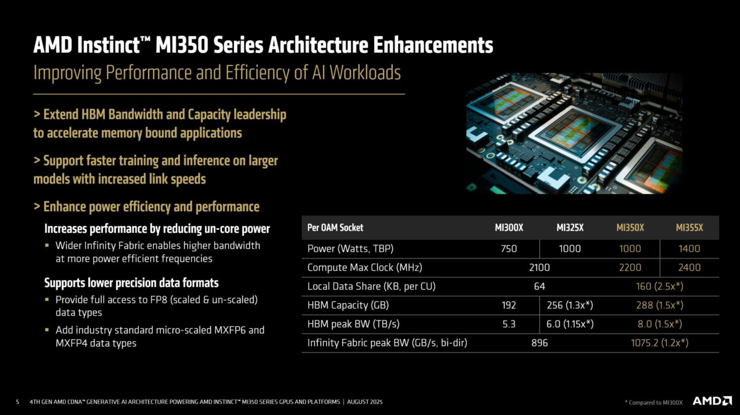
AMD detailed the their two upcoming Instinct series GPUs, the MI350X and the MI355X. As we detailed back in June, the two are almost identical in their memory and compute system designs. The only real difference of relevance to customers will be the TDP: the 350 at 1kW and the 355 at 1.4kW. The first is aimed at 8-GPU air cooled servers where datacentres prefer to stick to ~10kW per 6-8U of rack space, and the second is aimed at 4 or 8-GPU liquid cooled servers, where the power can reach 15 or even 18kW per 4-6U of space. For more info on the rack-scale setups and topologies, see Semianalysis' excellent article.
Oracle has already announced an order of over 130K MI355X GPUs for their upcoming zettascale AMD cluster, and other Hyperscalers and the AMD-centric neoclouds will no doubt be placing smaller orders. We could very well be seeing AMD taking a double digit market share from Nvidia soon if their software can improve fast enough to avoid the issues that prevented the rise of MI250X and MI300X GPUs.
To compare to the Blackwell series (1 2 3 4):
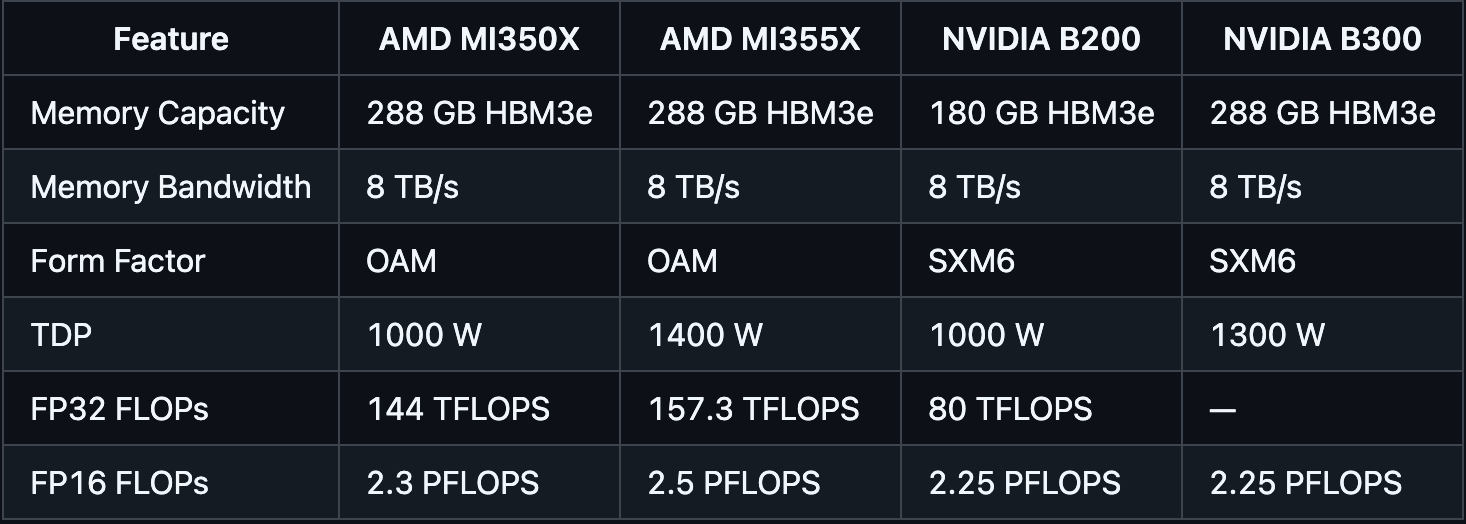
All FLOPs are given without sparsity - no idea why these vendors insist on giving 2:1 sparsity figures.
Memory capacity and bandwidth will now be on par, and compute numbers seem slightly better for FP16.
Source: AMD
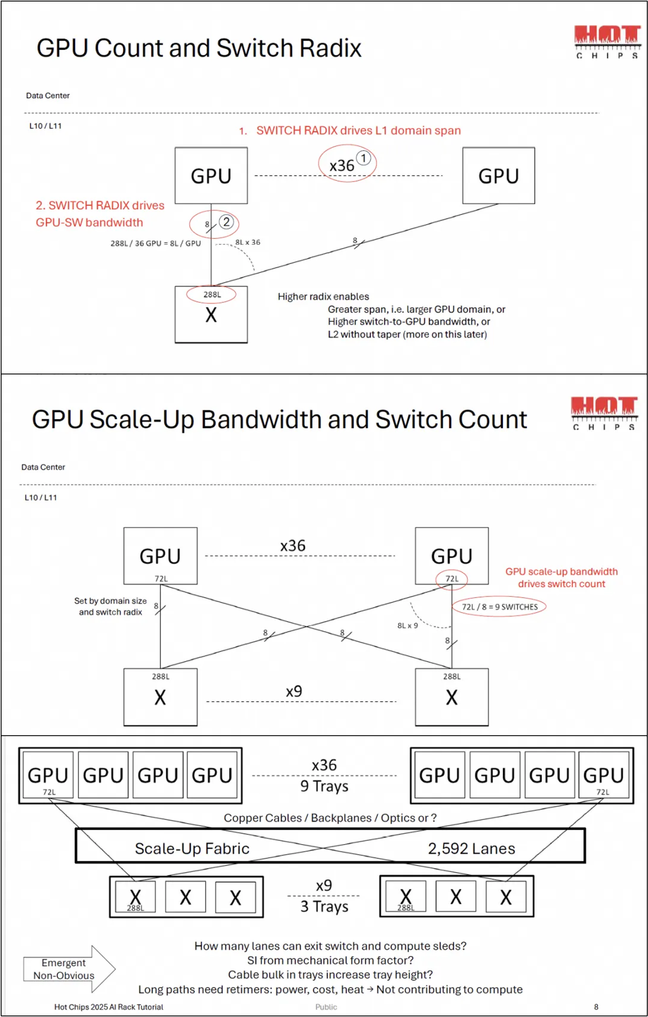
Their more scientific session was on the design of scale-up fabrics, where they discussed the effects that scale-up switch radix and device lane counts have on the size of the scale-up domain and its bandwidth. Of course, anyone can deduce that more links is better but AMD stressed that scale-up domains should be kept as a single-tier network. They proposed a 1.5 layer network that mitigates some of the issues described in the slides below too, which was quite interesting. More details in Zartbot's article on day 0 of HotChips 25.
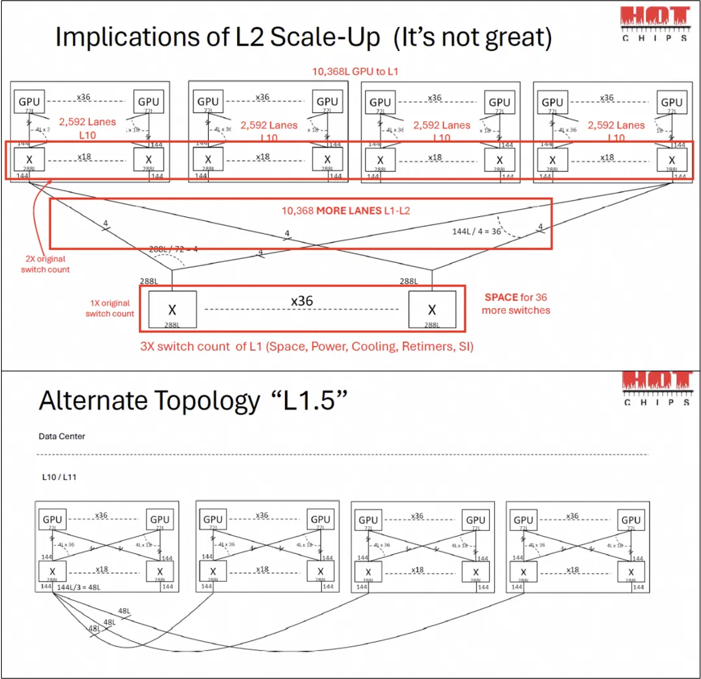
Source: AMD
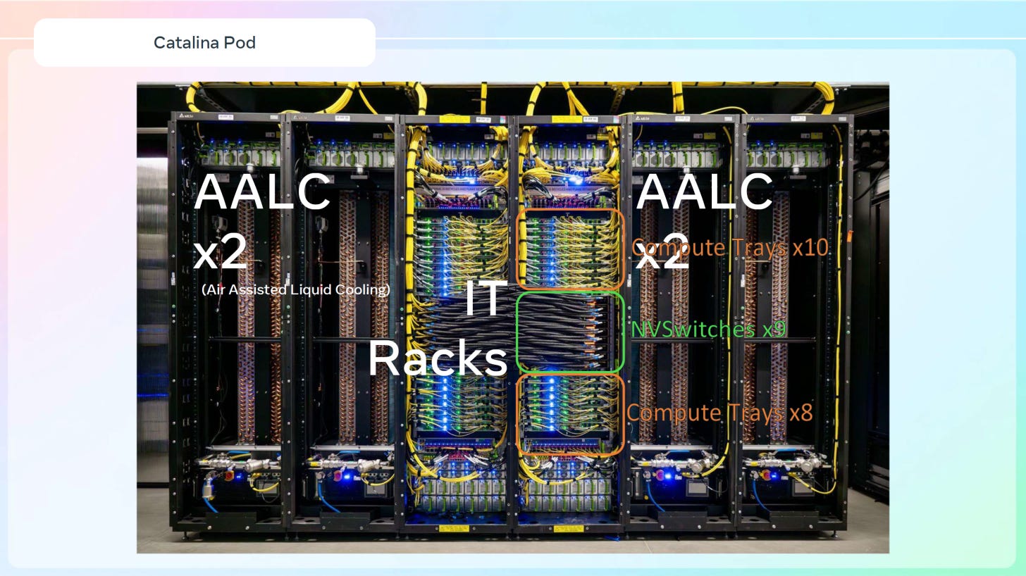
Meta: Catalina pod (NVL36x2)
One of the major issues with NVL72 systems when they were first announced was how few datacentres could at the time support such high power racks and how few could ever even hope to adapt their infrastructure to support them in the future. The NVL72 rack-scale form factor remains a non-starter for the majority of datacentres around the world, as most places support between 12 or 20kW per rack. This includes Meta, who have a lot of datacentre space designed for CPU servers and low-power MTIA accelerators.
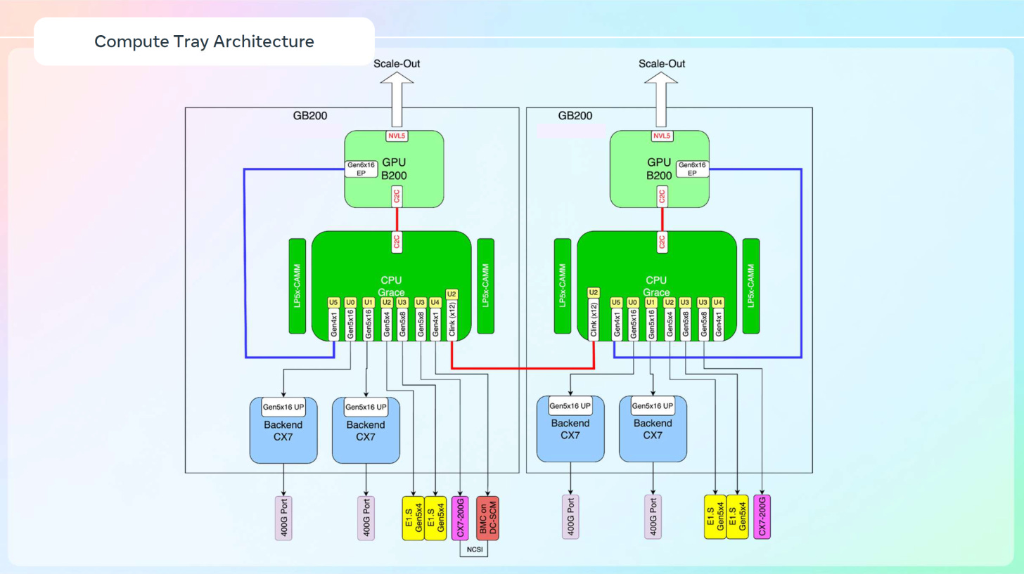
But for training their foundation models, Meta would prefer the raw bandwidth of the 72-GPU NVLink scale-up domain instead of the 8-GPU domain bounded by a chassis for HGX type servers. This, as well as other reasons, led them to customise the system to the extent that it became six racks.
The "Catalina" pod - a six-rack system designed to support 120kW of TDP over 6 x 20kW racks - brings 2 racks of 18 custom GB200 trays together with 18 NVLink switch trays to form a single 72-GPU domain. Four of the six racks are dedicated just to the cooling systems: air-assisted liquid cooling, using the large volume available of four standard width racks to keep liquid coolant temperatures down using fans.
Source: Meta
To this extent, they had to customise the trays to have 2 GPUs per tray instead of the usual 4 in a GB200 compute tray, making the ratio of CPU:GPU = 1:1. This then doubles the number of CX-7 NICs and Grace CPUs per GPU, leading to some very interesting specs:
72 B200 GPUs and 72 Grace CPUs
34.6TB aggregate LPDDR5X memory
48TB aggregate cache-coherent memory (CPU-GPU unified memory)
14.4TB/s aggregate Scale-out bandwidth
Source: Meta
One issue we believe Meta works around is the lack of power headroom here, with the total system being restricted to 120kW with little or no push beyond that. Combined with the fact that the number of CPUs, NICs, NVLink switches, and many other components have actually increased in number due to this setup, this will likely lead to throttling of the GPUs clock rates to stay within the 120kW envelope.
Intel: Clearwater Forest CPU
Earlier this year we reported on leaks regarding Intel's upcoming Diamond Rapids CPU, their "P-core" only processor aimed at high performance AI/HPC clusters. The counterpart to the "rapids" series of CPU is the "forest" series, aimed at more scalable and less intensive workloads like virtualisation, hosting, databases and so on. For their upcoming Clearwater Forest CPU, Intel decided to go with an official reveal.
The below image summarises the specs for a dual-socket setup, so halve the quantities (except the UPI) for a single-socket setup. Though knowing the target market of these CPUs, a single-socket setup may be unlikely, as virtualisation and web/app hosting servers are supposed to be as core-dense and energy efficient as possible.
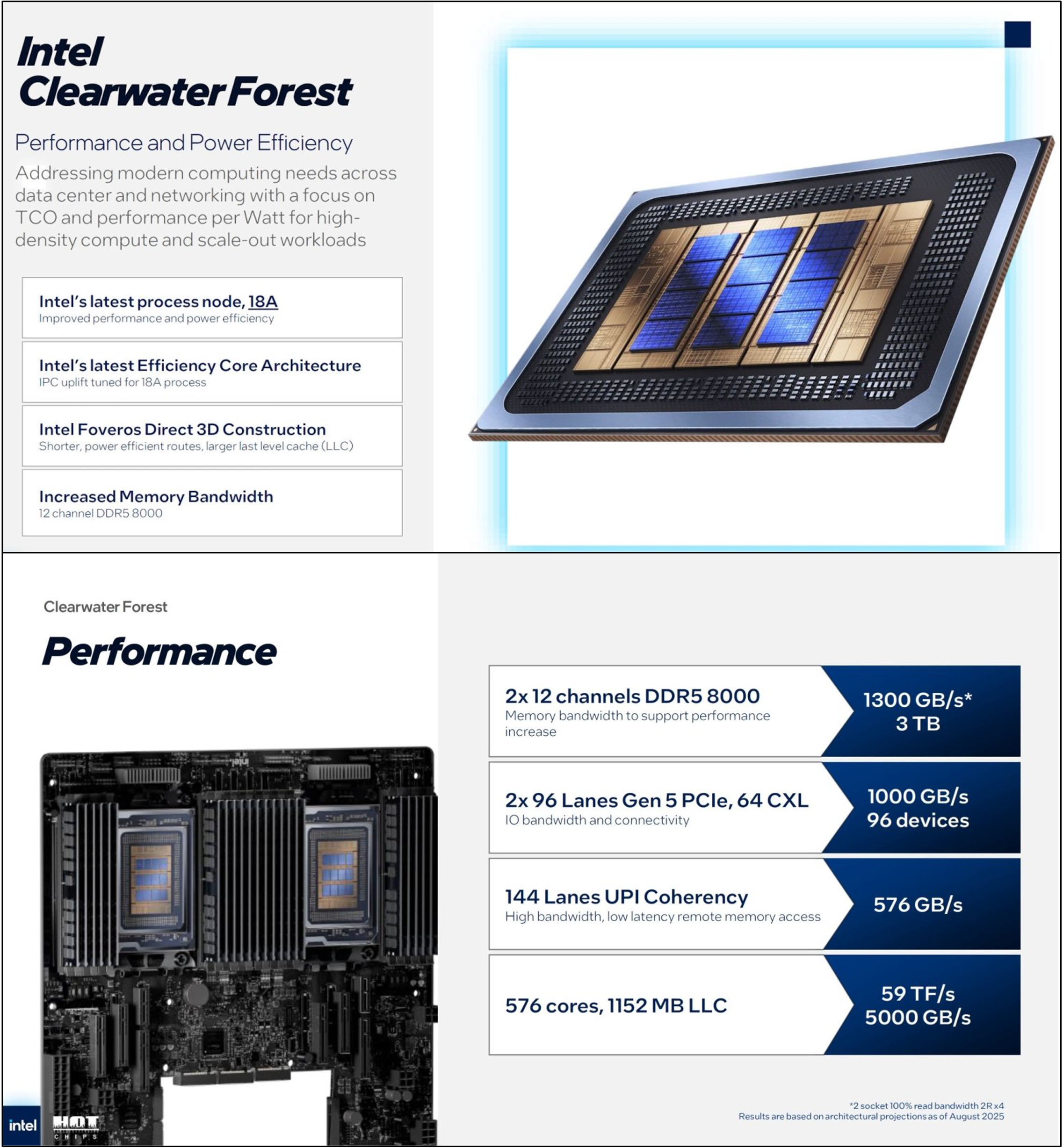
Source: Intel
For more information, Zartbot's article on WeChat and Andreas Schilling's article on HardwareLUXX are very detailed.
Others
There were also great sessions from names like d-Matrix, Rebellions, Marvell, Huawei, and more, but we wont cover them in this newsletter.
B300 GPU finally detailed
Also unveiled at HotChips 25 but given its own segment here, the B300 "Blackwell Ultra" GPU makes headlines even though most of the information given here was already known for months. We have a few details now though worth noting:
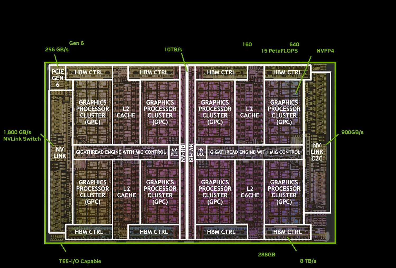
Source: Nvidia
288GB HBM3E is implemented as 8 stacks, probably at 12hi, totalling 8TB/s
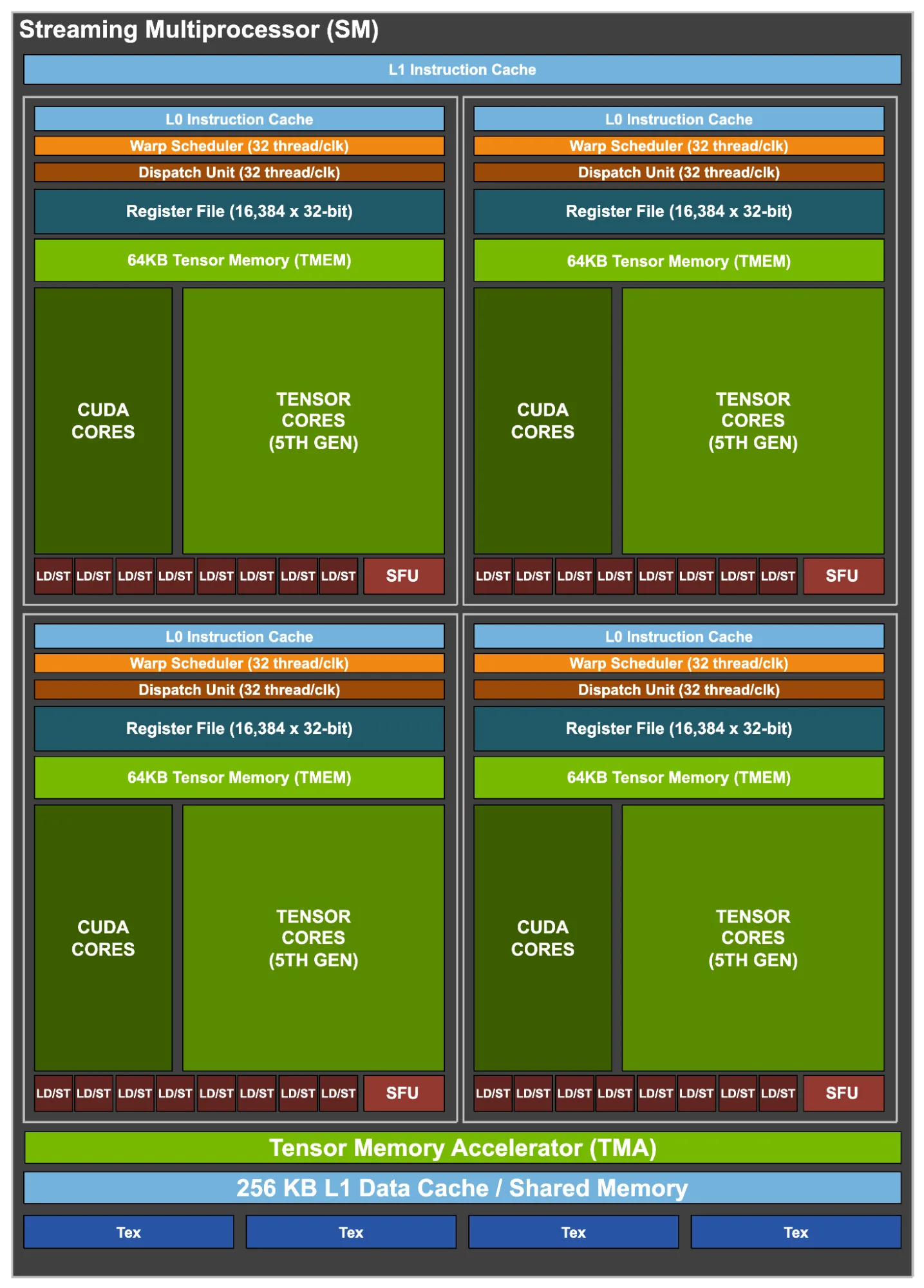
20,480 CUDA cores, and 160 streaming multiprocessors (SMs), which total to 640 5th gen. Tensor cores
Over 160MB of tensor memory (TMEM), the same volume of L1 data cache (shared mem), and L2 cache size unknown
Source: Nvidia
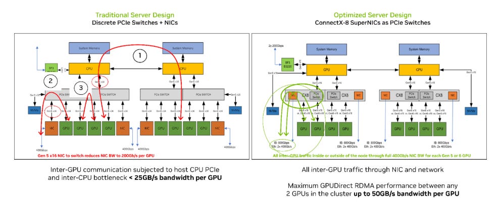
For more practical-minded people, the B300 sticks to the current generations 128GB/s unidirectional PCIe 6.0 x16 H2D connection, even though PCIe 6.0 CPUs or SSDs don't exist yet. PCIe 6.0 NICs, however, do exist, such as the ConnectX-8 SuperNIC with an integrated PCIe 6.0 switch. This marks a fundamental change in the server architecture for HGX's going forward, as GPUs now connect to the NICs at a 2:1 ratio instead of to discrete PCIe switches. This makes their connection to the scale-out network 1 hop shorter and also gives the GPUs a real chance to saturate the 800G uplinks. As for TDP, the peak of 1400W remains the same.
Source: Nvidia
Earlier this year, Nvidia developed the NVFP4 floating point format for efficient, stable, and accurate FP4 inference. The B300 delivers up to 1.5x the performance of the B200 for this format, but this is likely theoretical as actual NVFP4 quantised model inferencing numbers (tokens or samples per second) haven't been given yet. The majority of inferencing provided by foundation model labs as AI models or wrapped text or image generation services in other products may still happen on H100s and H200s though for a while. B300 customers investing in this hardware may do so for inferencing the largest models or for future proofing for the next year or two, or, most likely, training. This means that for many, NVFP4 performance numbers are irrelevant.
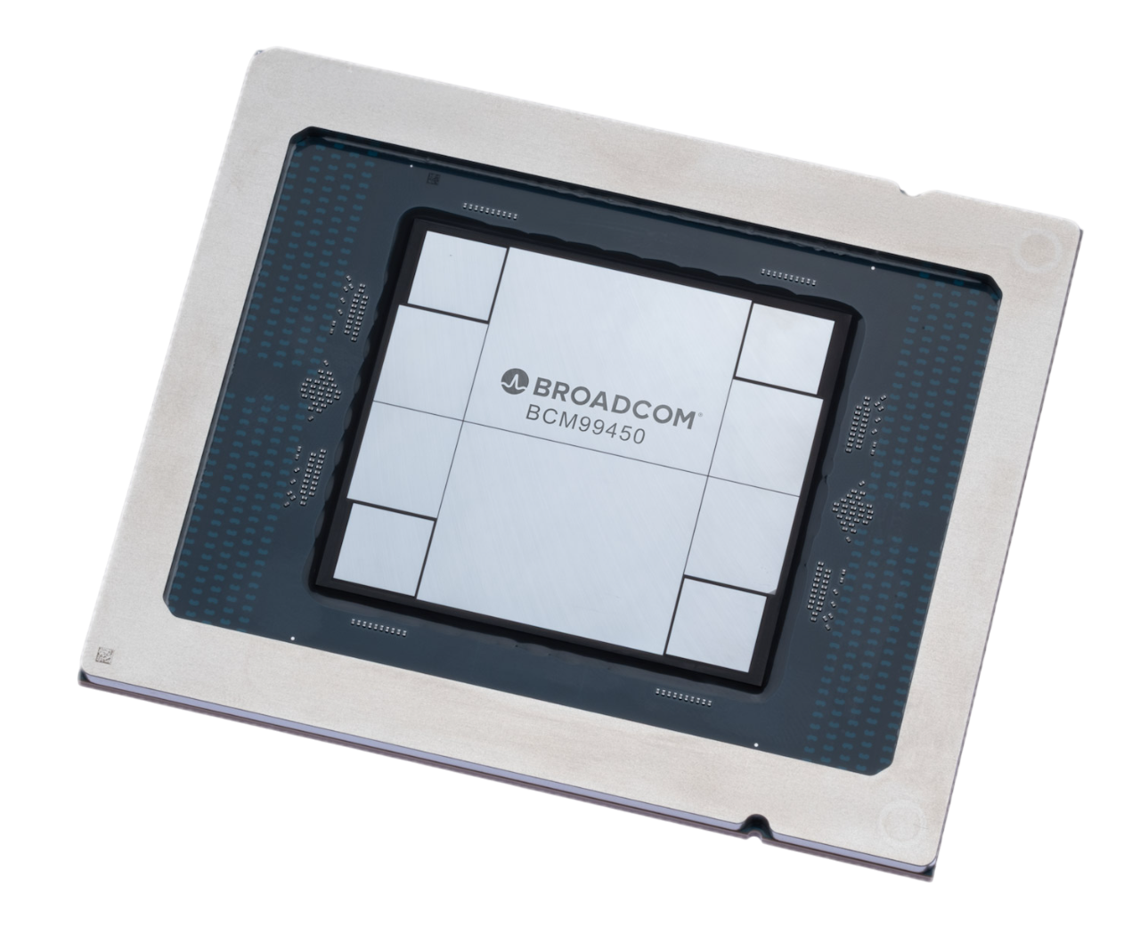
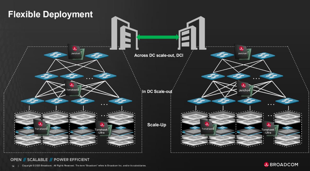
Yet another switch from Broadcom - scaling across with Jericho4
Scale-up and scale-out are both rapidly developing dimensions for device-device communications, though now we're beginning to see the limits of how far they can actually scale. Limits enforced not by the technology itself, but from cooling, power, and space constraints.
Racks, and even rows of racks can only get so big before the distance is too great for a larger scale out domain. Signal integrity and power become too difficult to manage beyond a few meters and taking scale-up to the optical domain is incredibly expensive. Though in certain markets like China, Huawei is showing that this might not be a roadblock to adoption.
Beyond that, scale-out can cover the span of a whole datacentre with a relatively high-bandwidth fabric, but after a certain scale, switch and optics costs become difficult to justify. Clusters like xAI's Colossus are pushing that boundary by doubling the size of the domain to 200,000 GPUs whilst keeping everything under a single scale-out ethernet fabric.
Source: Broadcom
Enter Broadcom, with the 51.2T Jericho4 "Across DC scale-out" ASIC. Aimed at long-range connections between scale-out fabrics (scale-out used synonymously with datacentre here), the Jericho4 includes many features that optimise for transport at these distances whilst maintaining a secure and lossless fabric.
Source: Broadcom
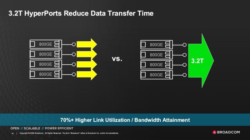
The main standout innovation that Broadcom advertise is the Hyperport - 4 x 800G links combined at the hardware-level into a single logical 3.2T port. This then reduces the associated overheads of managing 4 distinct ports too. This functionality has already existed for a while at the software layer with link aggregation (LAG) but Hyperport implements it lower in the stack, optimising the load balancing, congestion control, utilisation, and more.
Source: Broadcom
In addition, the Jericho4:
Has deep buffers to absorb bursty traffic from AI workloads
Supports lossless connections for over 100km distances
Provides MACsec at line rate, necessary for long-distance traffic
And just to future proof it for use in 2027/28, the Jericho4 is also UEC compliant - interoperable with all other UEC switches and NICs from any vendor.
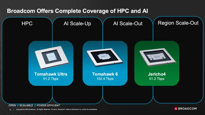
This then "completes" Broadcom's lineup of high-performance AI cluster switch ASICs, with this chip joining the Tomahawk 6 and Tomahawk Ultra to cover all three dimensions of network scaling: up, out, and across. For more information on the Tomahawk series, see our June and July editions.
Source: Broadcom
PS: It seems they'll do anything to avoid just saying "scale-across", perhaps to avoid association with Nvidia's Spectrum-XGS announcement (more on that just above)? Or maybe they were just a few days short to coining the term?
PCIe 8.0 announced
Intel and AMD's next generation CPUs - supporting PCIe (Peripheral Component Interconnect express) 6.0 - are expected to ship between 4Q25 and 4Q26, likely being followed closely by the corresponding SSDs, NICs, and more. PCIe 6.0 itself however was announced as early as 1Q22, resulting in a wait of over 3.5 to 4.5 years from announcement to implementation. Based on the pace so far demonstrated, future PCIe generations should take just as long to reach the market from their reveal. But there's been one fundamental addition to the world driving hardware progression to speeds not seen before: LLMs.
Keeping to their commitment to doubling bandwidth every 3 years, the PCI-SIG (Special Interest Group) has announced PCIe 8.0, aiming for up to 1TB/s bi-directional bandwidth over a full x16 connection. Version 1.0 of the specification is expected to be released in 2028, with the first devices hopefully shipping before 2032. In comparison, PCIe 7.0 was announced in 2022, aims to have it's version 1.0 ratified at the end of 2025, and may see adoption in devices as soon as 4Q26. Certainly not CPUs, but possibly in NICs (already reaching 800G and soon 1.6T), and just maybe in SSDs (if storage arrays and controllers reach those speeds in time).
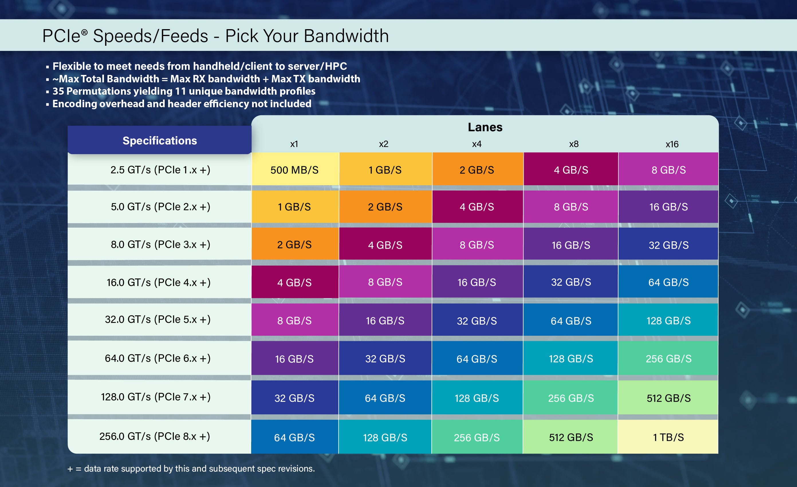
Source: PCI-SIG
To summarise what these speeds mean, PCIe 8.0 is targeting 256GT/s (Giga Transfers per second) bidirectional (both transmitting and receiving simultaneously) per lane. A lane is four wires, two each for transmitting (Tx) and receiving (Rx) and each pair is a differential pair. A transfer is 2 bits, since PCIe 8.0 will use PAM4 (pulse amplitude modulation with 4 levels) signalling. This means 512Gb/s per lane, or 64GB/s per lane, and therefore a x16 (full width) connection can support 16 x 64GB/s = ~1TB/s bi-directional bandwidth.
Other notable headlines
Jensen Huang confirms that GTC Washington DC will reveal the Rubin GPUs as well as five other chips
SK-Hynix to mass produce 2Tb 3D QLC NAND devices, on the path towards 244TB SSDs
Rumours of Nvidia's post-Rubin "Feynman" GPUs needing immersion cooling abound from industry sources
Huawei allegedly working on "AI SSDs" to reduce pressure on the Chinese HBM supply chain
...But SanDisk keeps up the pace by teaming up with SK-Hynix to work on standardising HBF first