

April 2025
AMD, Nvidia, and Huawei compete for the future.

(Want to see next month’s edition early? Follow this GitHub repo for the latest updates and early looks at the newsletter as it’s written - Also check out my LinkedIn!)
This month's updates:
SemiAnalysis on AMD's upcoming rack-scale SKUs
Tenstorrent announces the BlackHole AI accelerator
IBM's z17 mainframe
Ironwood: Google's seventh gen. TPU
China's answer to the NVL72 - Huawei's CloudMatrix 384
Other notable headlines
Vendor spotlight:
Kove
One-pagers:
Bandwidth and latency
Liquid cooling plates
This month's updates
SemiAnalysis on AMD's upcoming rack-scale SKUs
For AI accelerator manufacturers targeting hyperscalers, few things in AI hardware have become clearer in the past quarter than the need to focus now on systems rather than chips. Nvidia have taken the lead by supplying their NVL rack-scale products to all major hyperscalers as well as some GPUaaS providers, promising a turnkey infrastructure solution that meets the demands of the largest AI workloads. Rumours surface now of AMD's entry into this space with their own, the IF64 and IF128.
Historically, AMD have leveraged their strong partnerships with OEMs and integrators to build some of the worlds largest and most performant datacentre-scale systems, the most prominent recent example being the world's top-ranking supercomputer, El Capitan, built in collaboration with Cray (HPE). After the success of Nvidia's NVL systems though, AMD have moved to expand their own expertise in scaling beyond single servers through their acquisition of ZT systems, an integrator with extensive experience in building datacentre-scale systems with hyperscalers such as Azure and AWS. Now, reported exclusively by SemiAnalysis, IF64 and IF128 are likely to be the names of AMD's upcoming systems built around the MI450X GPUs and launching in 2H26.
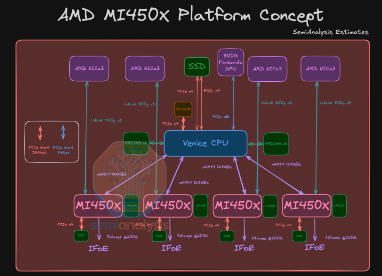
Nvidia's "Rubin" architecture GPUs (also planned for release in 2H26) are predicted to have a TDP of ~1.8kW and will be used in the "Oberon" fully liquid cooled NVL144 systems. The MI450X therefore may have a TDP of between 1.6 and 2kW to be competitive, and will likely also follow the industry trend of removing FP64 in place for native FP16 and FP8 support, though AMD may release a separate GPU dedicated for the Scientific/HPC applications in which the MI300X has shown great success. Again, similar to Rubin GPUs it's likely that each die of the MI450X will support a minimum of 288GB of HBM4, though unlike Nvidia, AMD will deploy its x86 EPYC datacentre CPUs rather than ARM-based low-power (and lower performance) Grace/Vera CPUs.
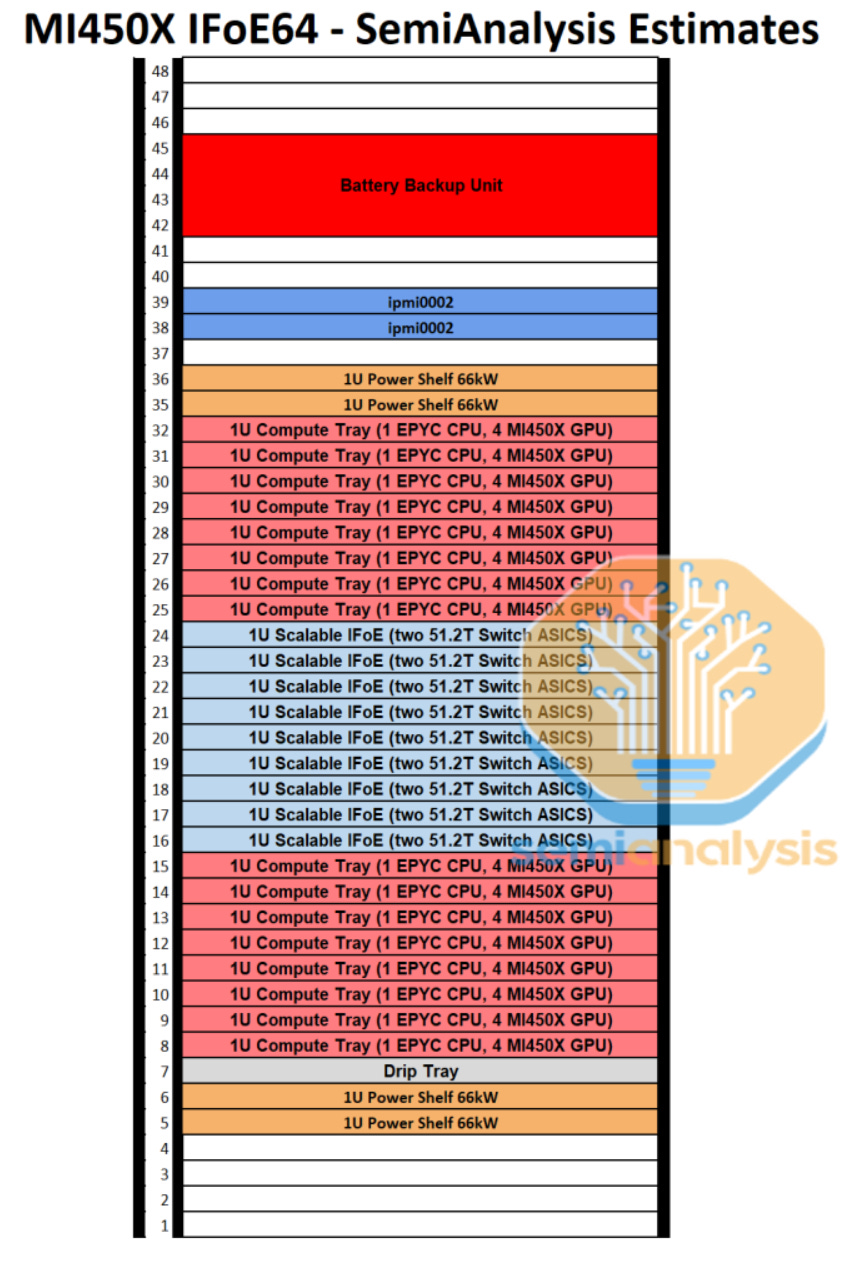
As for the scale-up network, AMD's Infinity Fabric over Ethernet (IFoE) likely just encapsulates the existing IF protocol already used for device-device (CPUs and GPUs) communication within a chassis and allows for it to be used over an ethernet fabric via NICs. SemiAnalysis predicts the performance of IFoE will allow for 1.8TB/s unidirectional bandwidth between GPUs, making it equivalent to the expected values for NVidia's 6th gen. NVLink. It's unclear what the maximum domain size will be and therefore how large a single system can get, but there are two key observations to note from the article: The first is that unlike Nvidia who cancelled theirs, AMD appear to be committed to a dual-rack DAC connected product (IF128), and the second is that from the B300 onwards, Nvidia will refer to a single die as a GPU rather than the entire package, leading to an artificial doubling of their GPU count.
Tenstorrent announces the BlackHole AI accelerator
American RISC chip/server design startup Tenstorrent seeks to take space in both the enterprise and retail AI accelerator markets with its low-power and easy to use PCIe card lineup, as well as servers designed around density and scaling. Their latest card, the BlackHole, seeks to offer a competitive price/performance ratio with a scale-up potential that appears to be significantly greater than what other PCIe devices from competitors such as Google and AWS can offer.
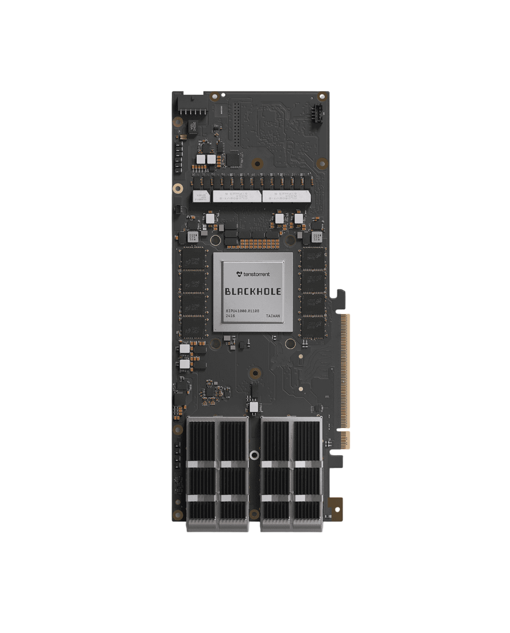
Run by industry legend Jim Keller, Tenstorrent is one of the many startups targeting the (relatively) low-power PCIe card AI accelerator space with the Wormhole, and now also the BlackHole cards. What makes Tenstorrent particularly unique is their custom IP for the RISC-V cores they use on their cards, designed specifically around their focus on keeping power draw low but also allowing for their "infinite" scaling strategy. The card comes in 3 forms, the P100a, p150a, and p150b, the first being a version without scale-up networking and only 28GB of GDDR6 with 120 RISC-V "Tensix" cores, and the last two being actively and passively cooled versions that come with scale-up ports on the PCB itself, as well as supporting up to 32GB of GDDR6 and 140 of the same cores.
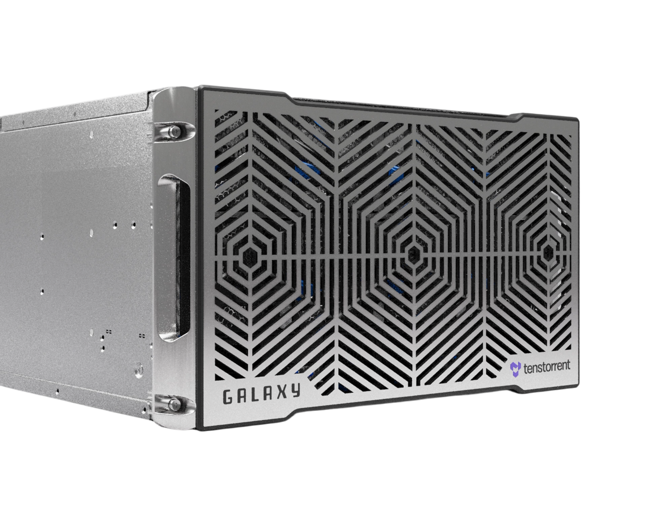
The Blackhole uses PCIe 5.0 for its host interface, but remarkably supports up to 3.2Tb/s of scale-up bandwidth through 4 x 800G QSFP-DD ports on the card itself. Some analysts suggest that due the sheer amount of bandwidth available on the card, it might even be usable as a network switch, though Tenstorrent clarifies that this interconnect will be exclusively for connecting to other Blackhole cards only. This p2p (peer-to-peer) scale-up strategy allows for creating 2D torus topologies much like Google's TPUs or AWS's Trainium cards and Tenstorrent's design of their server built around Blackhole cards, the "Galaxy", shows that they agree. A Tenstorrent Galaxy system contains 32 of the accelerators in a 6U chassis, arranged in a 4x8 mesh and providing up to 9.3 PFLOPs of FP8 performance in a 7.5kW envelope, leading to it being competitive against Nvidia's H100 HGX systems in efficiency (FLOPs/Watt).
IBM's z17 mainframe
IBM mainframes are known for their near perfect uptime and low-latency for critical operations such as transaction processing, airline fleet management, and fraud detection to name a few. As more and more such workloads begin to use computationally expensive AI models, IBM's mainframes need to adapt to not just be better at what they already do, but also be better at the workloads of the near-future.
The z16 mainframe released in 2Q22 was designed before transformer-based AI models had replaced many statistical/ML models in some mission critical applications, leading to IBM using the inbuilt AI acceleration capability of the Telum I processor to support such workloads. Integrated AI support came in the form of dedicated matrix units on the processors, but as the type and scale of AI workloads grew rapidly over the past 3 years, IBM realised that the next mainframe would necessarily need to be designed around AI workloads being run on dedicated accelerators. The z17 embodies this change, with the new system being designed to support AI workloads natively and with the same level of reliability and performance as other applications running on the mainframe.
As we reported in August last year, The Telum II and Spyre processors now used in the z17 are designed around extreme uptime, power efficiency, and consistent performance. The new mainframe hosts up to 32 Telum II CPUs, each containing 8 cores running at 5.5Ghz and 360MB of L2 cache, with 360MB and 2.8GB of virtual L3 and L4 caches respectively. The CPUs are supported by dedicated data processing units (DPUs) for offloading inter-processor communication and other functions for secure and reliable communications, leading to all 32 processors being connected in one scale-up I/O domain. Finally, the mainframe includes 12 I/O expansion drawers which can each support up to 16 PCIe Gen 5 cards, leading to a total of 192 Spyre AI accelerator cards - over 24TB of fast LPDDR5 memory - being installed in a single z17 system.
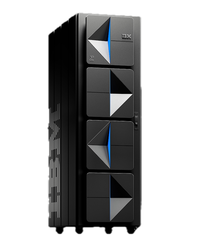
Holding true to their legendary eight nines (99.999999%) uptime guarantee, IBM openly discuss the development and testing process for their processors and systems showing how z17's will have around 1 second of downtime per year, even through up to magnitude 8.3 earthquakes. ServeTheHome's articles and review (1 2 3) reveal just how extensive IBM's development processes are, showing the complete vertical integration of their manufacturing and testing, from the materials and chemicals used for the processors and cooling systems to the racking and securing of the components for functionality under extreme conditions.
Ironwood: Google's seventh gen. TPU
In 2Q24 Google introduced the "Trillium" TPUv6 (Tensor processing unit), a continuation of their remarkably power-efficient series of custom AI accelerators available on GCP (Google cloud platform). Now, the series continues but with an unexpected progression: Inference and training are no-longer being assigned to two different versions in the same generation. The "Ironwood" TPUv7 appears to take on both workloads but the marketing around it confuses many.
Google's latest in their custom silicon for AI workloads, the "Ironwood" TPUv7 has just been announced. It's unclear yet what stage of production it's at, or when it will be generally available for public GCP users, but some specs are available now. Of all the information provided, the most controversial statement made was a misguided (or even dishonest) comparison between a TPU "pod" and the worlds most computationally capable supercomputer, El Capitan.
The "Top500" organisation maintains a list of the worlds most powerful supercomputers ranked by their performance in a linear algebra benchmark, Linpack. El Capitan, placing first as of 4Q24, combines over 43,000 AMD MI300A APUs (CPU + GPU on the same package) to achieve a real performance of 1.74 exaFLOPs at FP64, with a theoretical peak at 2.74. TPUv7 pods on the other hand use their 2 or 3-dimensional torus network topology to combine 9,216 chips (not devices) into a single computational domain. Additionally, the performance per chip provided in the announcement is a theoretical peak as opposed to a measured benchmark and is very likely for FP8 or FP16 as opposed to FP64. Google's claim therefore of reaching a 24x advantage in exaFLOPs over El Capitan has been received poorly by analysts with opinions generally skewing towards it being grossly misleading.
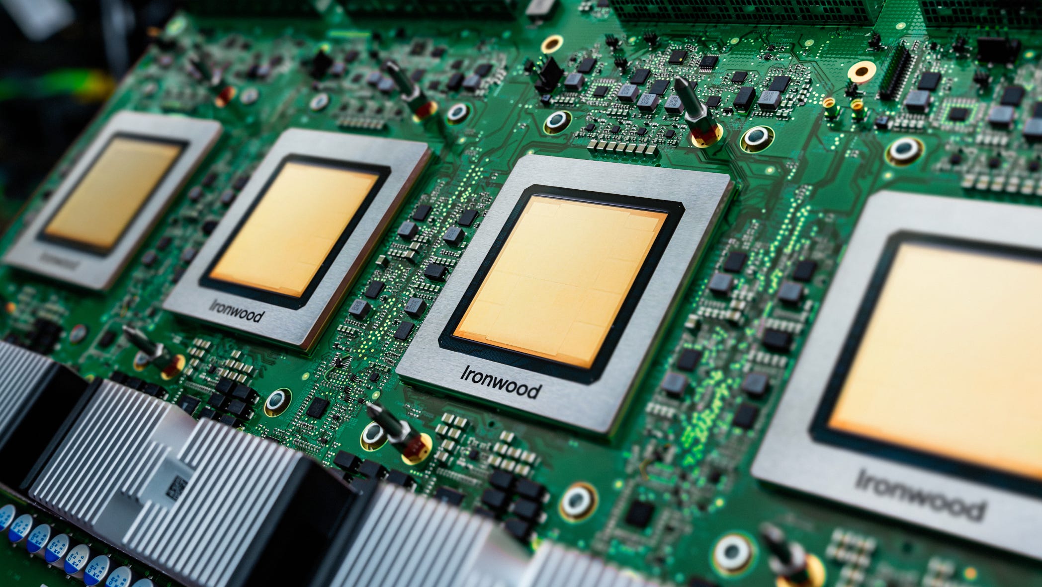
Focusing on the chip itself, it appears that the v7 is a natural successor to the v5p, the "performant" version of the 5th generation which aimed to handle both lighter inferencing workloads as well as AI model training use cases, (in contrast to the v5e or "efficient") rather than the v6 which was likely focused on inferencing only. Finally, looking at the specs (1 2 3 4):
4614 TFLOPs at FP8 (~2300 BF16)
192GB HBM at 7.2TB/s - likely 6 stacks of Micron's 12hi HBM3E
Likely 4 (possibly 6) ports of ICI at 1.2TB/s bidirectional
ICI domain size of 9216, possibly in a 96x96 2D torus or 32x32x9 3D torus
4 x 256x256 MXU (systolic arrays), providing 65536 MACs/cycle
Estimates of up to ~1kW per chip
China's answer to the NVL72 - Huawei's CloudMatrix 384
Nvidia's NVL72 was not the first but was certainly the most popular rack-scale, self-contained infrastructure solution built around AI accelerators. Densely packing this volume of high-powered chips into a single rack and interconnecting them with the NVLink scale-up network led to a product that could be easily integrated and used by hyperscalers and large businesses. But the NVL72 has its flaws, and Huawei is stepping up to take on Nvidia in this space too.
It's likely to come as a surprise to many who don't operate in the Chinese market, but Nvidia internally see Huawei as one of their biggest competitors for AI accelerators. We reported back in February and even last October about Huawei's progress in high-performance AI accelerators, with their Ascend 910C being announced and now mass produced for use in firms such as Baidu, ByteDance, and most famously, DeepSeek. All interested parties were or are evaluating the chips in hopes of beginning to taper off of their reliance on foreign hardware amidst increasingly hostile export policies from the US.
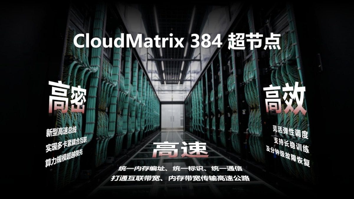
Seeing the trend in the market for rack-scale systems, Huawei have announced their own reference architecture, the CloudMatrix (CM) 384, a multi-rack system built around the Ascend 910C AI accelerators and "CloudEngine" network switches. The 16-rack, 384 chip SKU hosts 4 x 8-GPU air-cooled servers per rack over 12 racks with 4 racks of switches, and is fully optically connected for its single scale-up domain; this means that unlike the NVL72 which uses copper for its NVLink scale-up network, the CM384 uses almost 5400 400G transceivers. Some analysts predict that this fact alone will limit the number of CM384s that will ever be deployed as its possible that the supply of transceivers will be insufficient to meet the demand for the racks. Others raise concerns about the total power draw of the system being a hindrance to its adoption, predicted to be at ~560-600kW per unit, well over 3x the advertised power of the NVL72. Despite this, SemiAnalysis' calculations show an advantage in the FLOPs/Watt ratio of the CM384 over the NVL72, also noting that power availability is usually not an issue for datacentres in China as it is in the US and Europe.
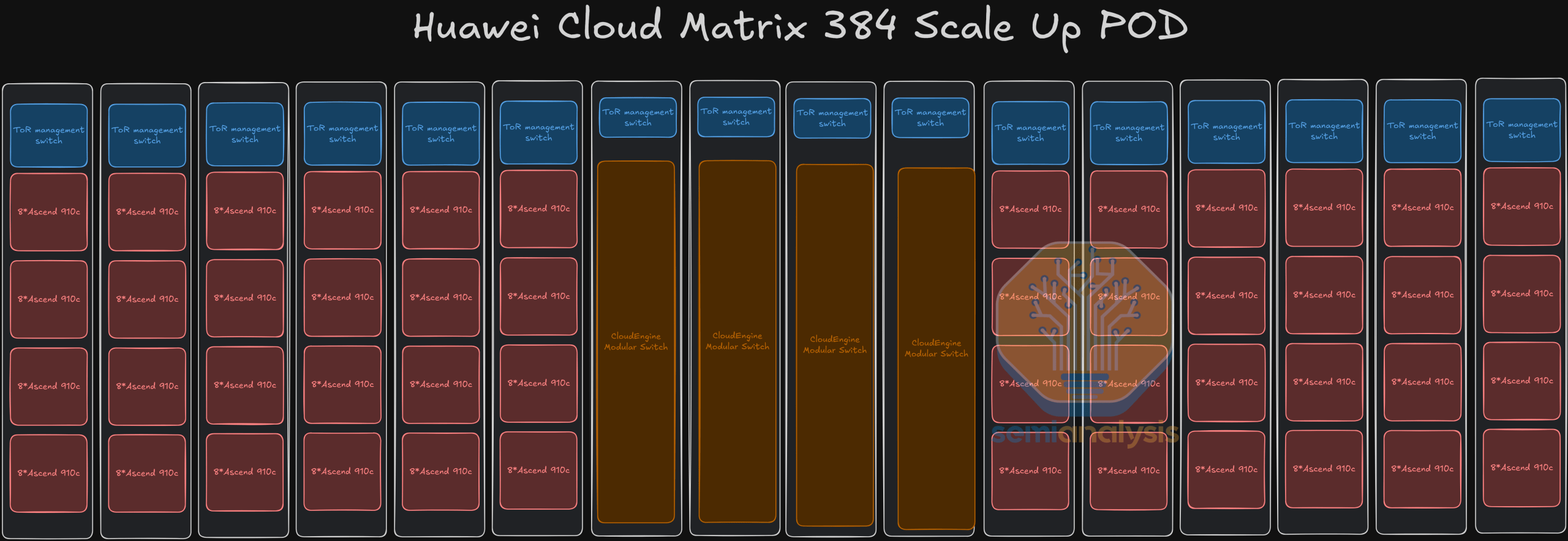
As for the system's specs (1 2):
~300 PFLOPs at BF16, ~780 TFLOPs per chip
49.2TB of HBM total, 128GB per chip
~1 PFLOPs aggregate unidirectional scale-up bandwidth
~150 TFLOPs aggregate unidirectional scale-out bandwidth
~600kW TDP at peak load with all transceivers in
Other notable headlines
SK-Hynix possibly mass producing both HBM4 and HBM4E this year
Chinese firms place up to $16 billion of orders for Nvidia's CHIPS act-dodging AI GPUs
Samsung reportedly begins developing its 1nm "dream" process, ready for mass production in 2029
Intel confirms experiments on direct-liquid cooled solutions for CPUs reaching up to 1000W TDPs
Vendor spotlight
Kove
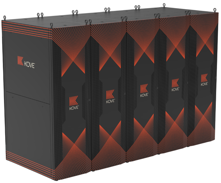
Host memory capacity is and has always been the be-all and end-all of large, high-performance workloads, as triggering an OOM error usually causes not just the application and its progress/state to crash, but the entire host. Kove are a firm working to change this with a solution for remote, software-defined memory (SDM) that approaches the performance of local memory.
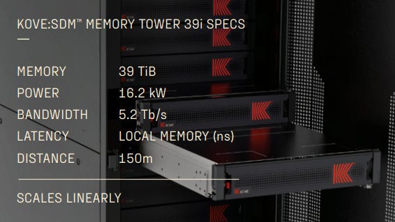
Founded in 2003, American firm Kove has quietly been supplying remote memory solutions to customers who found their workloads constrained not by compute, but by memory capacity. Kove's memory tower system presents as a rack of DRAM enclosures containing some management compute and high-performance NICs, and their software stack manages the remote memory and transfers to expose a memory pool that can be defined (configured or managed) entirely by software. With a maximum capacity of up to 256TiB (tebibyte, or 2^40 as opposed to 10^12 bytes) across several memory towers available as one unified address space with the local memory, bandwidth-intensive workloads can be accelerated without needing the compute to be throttled.
At a high-level, the memory tower works by extending the main memory available to a host machine via network-attached DRAM, rather than adding more channels for DIMMs onto the host baseboard or connecting another board via PCIe. Kove supports InfiniBand for the data plane (with RoCE support in the works) and Ethernet for the control plane, allowing for reasonably easy to manage additional infrastructure in any standard ethernet-managed datacentre with a dedicated and isolated high-performance fabric for the data.
As for software, the management and networking stack works together to use a host server's local memory as a form of cache (think of it as L4/5), and keeps recently accessed and likely soon to be accessed within the host chassis. Remote memory then is able to serve as a nearly-identical access latency extension of this local cache, as the microseconds of time to RDMA data from the tower to host are likely amortized away by both the large bandwidth available on the network and the access prediction capabilities of the software.
One-pagers
Bandwidth and latency
Bandwidth, being the amount of data transferred within a unit time and latency, being the time taken to complete a transfer of a unit size, these two key measurements in any data transfer are often misunderstood and misrepresented. Even worse, some will simple invert bandwidth and call it latency not realising their lack of consideration for overheads, measurement conditions, and variance, and the damage they do to the science.
Measuring the performance of transferring data via a connection is usually done with two measurements: bandwidth and latency.
Bandwidth measures the maximum volume of data that can be transferred through a connection in a given unit of time, and is measured as a rate such as Mbps (megabits per second). It's important to note that this is the maximum theoretical rate, not the actual or "realised" rate of data transfer across a connection. Bandwidth is often abstracted (applied to) or aggregated (accumulated) across a subset or an entirety of a network to give some indication of the potential rate that can be achieved for a workload using it. Latency on the other hand measures the time taken for a minimum unit volume of data to be transferred from a source to a destination, and is measured in units of time such as milliseconds. Some factors that influence latency like distance between endpoints or the speed/path of light in a material are physical and unavoidable, whilst others like the time to encode and decode signals are dependant on the hardware and protocols used for transmission.
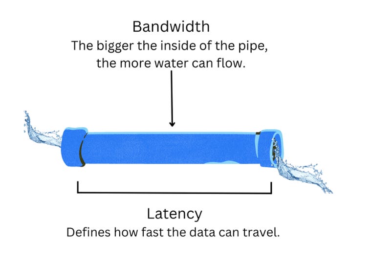
A common error made when measuring network performance is assuming that bandwidth is the inverse of latency, i.e. that a bandwidth of 100 Mbps implies a latency of 1/100 seconds. This assumption ignores a few issues:
Latency is only measured for a minimal sized transfer, one that should never be large enough to saturate a link for measuring bandwidth
Bandwidth does not include the overheads involved with each minimal transfer, as these are amortized away when sending data in volume
As the rate of transfer over w channel increases, so does contention and hence resource utilisation, which causes an increase in latency i.e. the relationship is non-linear
Liquid cooling plates
The height of air-cooled AI servers is influenced significantly by the size of the fans and the height of the heatsinks required to keep high-powered accelerator hardware cool. Compression attached cooling plates replace tall towers of metal fins in thinner-profile servers where getting enough airflow for cooling kilowatt+ devices either costs double-digit percentages of the servers total power draw, or is just physically impossible.
A prime example of air cooling pushed to its limits is SuperMicro's B200 HGX server, the SYS-A22GA-NBRT. Fitting 8 Nvidia B200 GPUs (each with a TDP of 1200W) as well as 2 Intel Xeon 6900s (about 500W each) into an air cooled chassis requires accommodating the cooling fin towers for the GPUs, taking up the entire floor-space in the chassis as well as over 6U of height. The remaining space needs to be large enough so that enough airflow can pass to keep the other components such as CPUs, NICs, SSDs and more. Pushing beyond this limit to 1400W+ TDP chips and more will require significantly greater volumes of airflow moving through impractically large chassis, to the point where the power used by cooling fans will creep towards 15 or even 20% of the servers total draw.
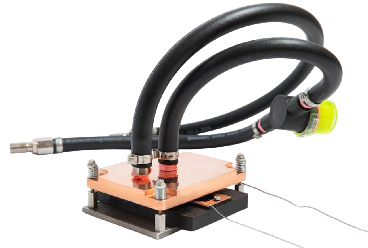
Using a denser fluid such as liquid is the next logical step for cooling systems. Immersion cooling appears to still be building a reputation, having been only applied successfully in a very small number of setups, and so the only practical solution currently is direct-to-chip liquid cooling. In this paradigm, large coolant distribution units (CDUs) are placed underneath or at the side of existing racks and large, high pressure plumbing systems connect the pumps to in/outlets on the chassis. Further plumbing internal to the chassis then routes the cooled liquid from the CDU through "cold plates", or flat hollow plates made from copper or aluminium, which are in placed in contact with the chips/components. The heated liquid is then pumped back to the CDU for cooling.
Systems like the plate shown above can reliably cool chips with TDPs of up to 2000W, with models rated for 4000W (under very high coolant pressures) being evaluated for future AI accelerators. For servers, adopting cooling plates for all or even some of the components leads to a significant increase in power efficiency and compute density, allowing for solutions like Nvidia's NVL72 racks. Definitely not the first - but by far the most popular - NVL72s use extensive liquid cooling support infrastructure to cool 27 x 1U trays in a single rack, requiring many types of cooling plates for the various collections of components on the baseboard. Moving forward, more standard server architectures are likely to shrink in size towards 2-4U and datacentre PUE values will decrease.